
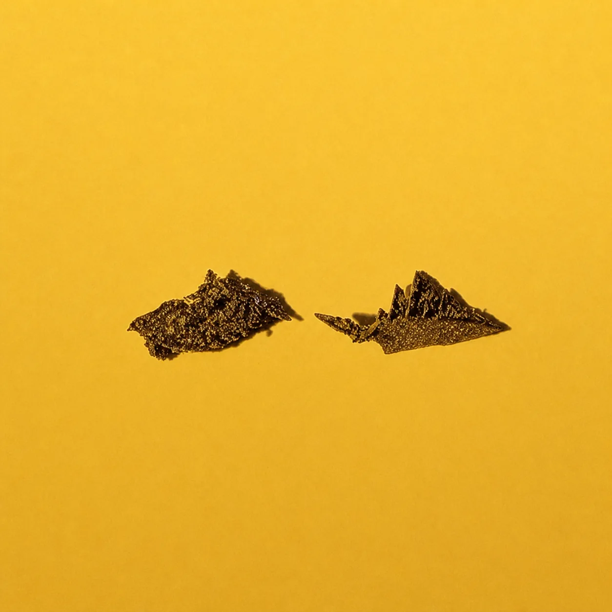
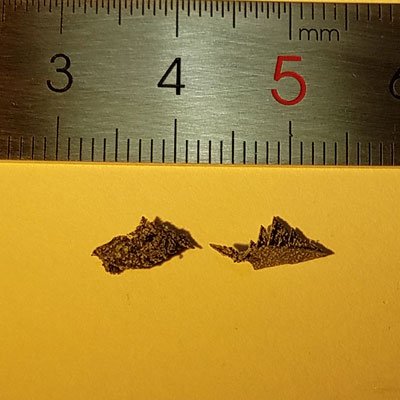
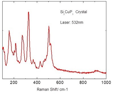
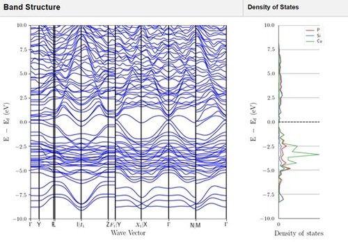
Si₂CuP₃ Crystals
Si₂CuP₃ is a layered ternary phosphide material with a van der Waals structure, has its semiconducting behavior, strong optical absorption, and high thermal behavior. Its unique combination of properties makes it applicable to applications in optoelectronics, thermoelectrics, and quantum materials research.
Sample Size Options:
Crystals larger than 10 mm²
Crystals larger than 25 mm²
Crystals larger than 100 mm²
Material Properties:
Layered van der Waals Structure: Facilitates exfoliation into monolayers or few-layer sheets for 2D material studies.
Semiconducting Behavior: Moderate bandgap applicable to optoelectronic and thermoelectric devices.
High Thermal behavior: High behavior under ambient and high-temperature conditions.
Optical Absorption: Strong absorption in the visible spectrum for photonic applications.
Crystal Structure:
Type: Layered structure with van der Waals interactions
Features: Easily cleavable layers for thin-film fabrication and nanoscale studies.
Degree of Exfoliation:
Ease of Use: Readily exfoliates into thin layers for specialized research and applications.
Other Characteristics:
Thermoelectric Efficiency: Promising for energy conversion and waste heat recovery.
Optoelectronic Potential: Applicable to standard photodetectors and light-sensitive devices.
Quantum Research Opportunities: Permits exploration of electronic and transport phenomena in layered systems.
Applications:
Optoelectronics:
Applicable for photodetectors, light-emitting diodes, and photovoltaic devices. Thermoelectric Devices:
Applicable to energy harvesting and thermal management systems. Quantum Materials Research:
Promising for studying electronic transport and quantum effects in layered phosphides.
2D Material Studies:
Applicable for assembly into van der Waals heterostructures and thin-film devices. Energy
Applications:
High potential for thermoelectric and catalytic applications. Synthesis Method:
| Option 1 | > 10 mm², > 100 mm², > 25 mm² |
|---|
Related products
-
HOPG
$668.25 -
ZrTe₃ Crystals
Price range: $696.09 through $835.32 -
MoTe₂ Crystals (2H phase)
Price range: $696.09 through $793.55 -
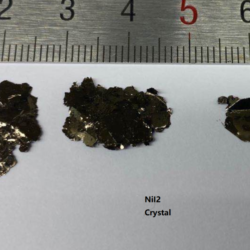
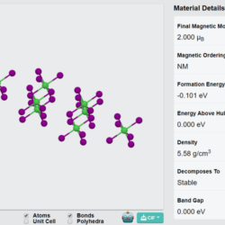
NiI₂ Crystals
Price range: $696.09 through $1,390.81 -
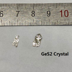
GeS₂ Crystals
Price range: $696.09 through $835.32 -
Co₃Sn₂S₂ Crystals
$835.32 -
Ni₂Bi₂Te₅ Crystals
Price range: $696.09 through $793.55 -
WSeTe Crystals
Price range: $835.32 through $1,252.98 -
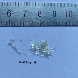
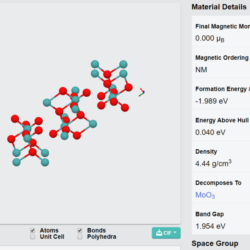
α-MoO₃ Crystals
Price range: $640.41 through $696.09 -
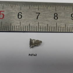
PdTe₂ Crystals
$696.09