
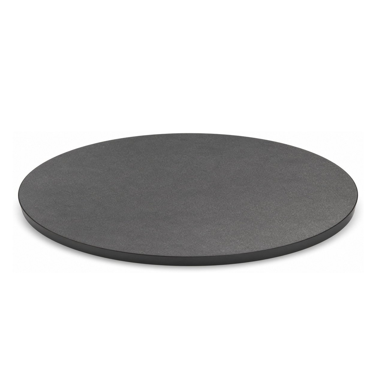
Lead Telluride (PbTe) Sputtering Target, 99.999% (5N) Purity, Circular (Price Upon Request)
Price upon request
Lead Telluride (PbTe) Sputtering Target, 99.999% (5N) Purity, Circular (Price Upon Request)
Lead Telluride (PbTe) sputtering target is a narrow-bandgap compound semiconductor PVD source material for magnetron sputtering, ion sputtering, and laboratory thin-film deposition. It is supplied in circular target formats for research, development, and small-batch process work where controlled handling, stated dimensions, and material identity are specified. Pricing for this material is provided upon request because final cost depends on current material market conditions and selected dimensions.
Features
Source Material
Supplied at 99.999% (5N) purity for thin-film workflows that require controlled source composition for deposition work.
Circular Target Formats
Available in circular diameters including 2 inch diameter (50.8 mm), 2.36 inch diameter (60 mm), 3 inch diameter (76.2 mm). Thickness options include 3 mm thick, depending on the selected diameter and target configuration.
Controlled Processing and Inspection
Target preparation may include material selection, forming, heat treatment, precision machining, dimensional inspection, surface finishing, cleaning, and final inspection. Composition and impurity control may be supported by analytical methods such as ICP, GDMS, carbon/sulfur analysis, oxygen/nitrogen analysis, and metallographic inspection where appropriate.
Controlled Handling and Packaging
Targets are prepared for deposition use with controlled surface handling and protective packaging. Store sealed in a dry environment, handle with gloves, and avoid direct contact with oil, dust, moisture, or other surface contamination before installation.
Technical Specifications
Material: Lead Telluride (PbTe)
Purity: 99.999% (5N)
Form: Circular sputtering target
Available Diameters: 2 inch diameter (50.8 mm), 2.36 inch diameter (60 mm), 3 inch diameter (76.2 mm)
Available Thicknesses: 3 mm thick
Compatible Equipment: Single-target sputtering systems, multi-target sputtering systems, ion sputtering systems, and magnetron sputtering equipment
Packaging: Protective target packaging for laboratory shipment and storage
Common Applications
– thermoelectric thin-film research; infrared detector material development; narrow-bandgap semiconductor coatings; compound semiconductor PVD studies
– Academic, industrial, and pilot-scale thin-film process development
| Option 1 | 99.999% (5N) |
|---|---|
| Option 2 | 2 inch diameter (50.8 mm), 2.36 inch diameter (60 mm), 3 inch diameter (76.2 mm) |
| Option 3 | 3 mm thick |
Related products
-
-
-
Copper (Cu) Sputtering Target, 99.995% Purity, Circular
Original price was: $115.54 – $247.80Price range: $115.54 through $247.80. Price range: $104.40 through $222.74Current price is: $104.40 – $222.74Price range: $104.40 through $222.74. Hot -
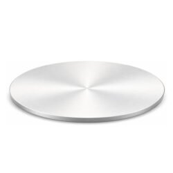
Aluminum (Al) Sputtering Target, 99.999% (5N) Purity, Circular
Price range: $164.27 through $492.83 -
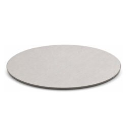
Cobalt (Co) Sputtering Target, 99.95% (3N5) Purity, Circular
Price range: $158.70 through $456.63 -
-
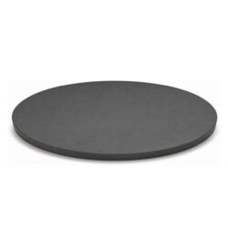
Niobium Nitride (NbN) Sputtering Target, 99.9% (3N) Purity, Circular
Price range: $1,073.38 through $2,386.24 -
Chromium (Cr) Sputtering Target, 99.95%-99.99% Purity, Circular
Price range: $150.35 through $693.31 -
Copper (Cu) Sputtering Target, 99.99% (4N) Purity, Circular
Price range: $147.56 through $199.07 -
Copper (Cu) Sputtering Target, 99.9995%-99.9999% Purity, Circular
Price range: $208.82 through $676.60