
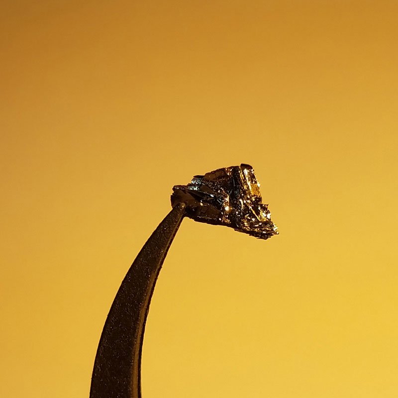
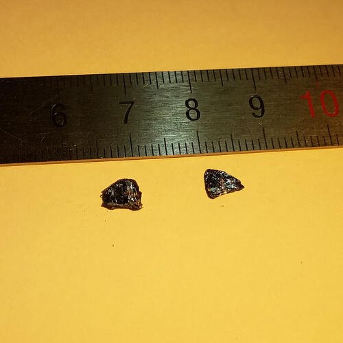
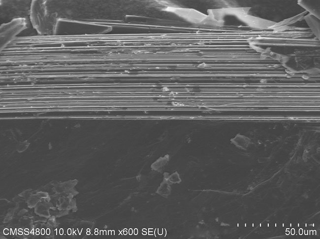
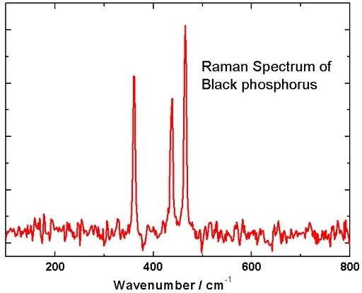
Black Phosphorus Crystals
Black Phosphorus (BP) is a layered semiconductor with a puckered orthorhombic structure, exhibiting strong anisotropic electronic, optical, and thermal properties. Its direct bandgap, which is variable from ~0.3 eV (bulk) to ~2.0 eV (monolayer), makes it a highly applicable material for applications in optoelectronics, photonics, energy storage, and 2D materials research. Our Black Phosphorus crystals are synthesized using the Chemical Vapor Transport (CVT) method, with high purity, precise stoichiometry, and high crystallinity.
Sample Size Options:
Crystals larger than 10 mm²
Crystals larger than 25 mm²
Crystals larger than 100 mm²
Material Properties:
Layered van der Waals Structure: Facilitates easy exfoliation into monolayers or few-layer sheets.
Variable Direct Bandgap: Ranges from ~0.3 eV (bulk) to ~2.0 eV (monolayer), making it applicable for variable optoelectronic applications.
High Carrier Mobility: Exhibits electron mobility above 1,000 cm²/V-s at room temperature.
Anisotropic Properties: Strong in-plane anisotropy in electrical, thermal, and optical behavior.
Crystal Structure:
Type: Orthorhombic puckered layered structure
Features: Cleavable layers, applicable for thin-film fabrication, nanoscale research, and device assembly.
Degree of Exfoliation:
Ease of Use: Easily exfoliated into monolayers or few-layer nanosheets for 2D materials research and device applications.
Other Characteristics:
Environmental Sensitivity: Requires inert conditions for storage and handling to prevent degradation.
Photothermal Performance: High potential for photothermal conversion and infrared detection.
Quantum Confinement Effects: Exhibits unique quantum phenomena when thinned down to monolayer form.
Applications:
Optoelectronics:
Applicable for photodetectors, light-emitting diodes (LEDs), and variable photovoltaic devices. Field-Effect Transistors (FETs):
Standard material for flexible, low-power, and high-speed electronic devices. Quantum Materials Research:
Applicable to exploring quantum confinement effects and anisotropic electronic transport.
2D Material Studies:
Applicable for assembly into van der Waals heterostructures and flexible electronic systems. Energy
Applications:
Potential for lithium-ion batteries, supercapacitors, and photothermal energy conversion.
| Option 1 | > 10 mm², > 100 mm², > 25 mm² |
|---|
Related products
-
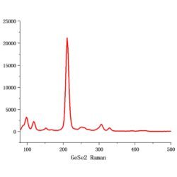
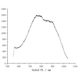
GeSe₂ Crystals
Price range: $696.09 through $793.55 -
WSeTe Crystals
Price range: $835.32 through $1,252.98 -
FeBr₃ Crystals
Price range: $654.33 through $696.09 -
FeCl₃ Crystals
Price range: $696.09 through $1,252.98 -

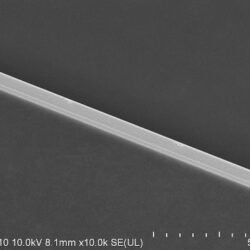
MoTe₂ Crystals (2H phase)
Price range: $696.09 through $793.55 -
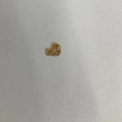
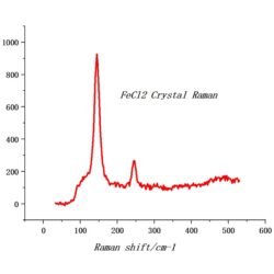
FeCl₂ Crystals
Price range: $696.09 through $793.55 -

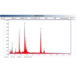
Co₃Sn₂S₂ Crystals
$835.32 -
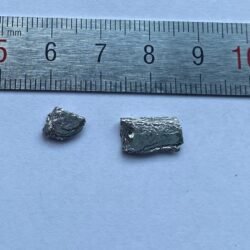
Ni₂Bi₂Te₅ Crystals
Price range: $696.09 through $793.55 -
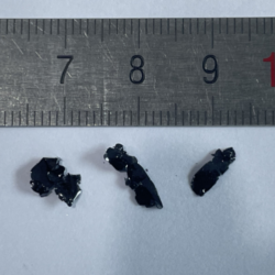
RuCl₃ Crystals
Price range: $696.09 through $1,252.98 -
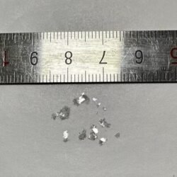
BiOCl Crystals
Price range: $696.09 through $793.55