
GeSe Crystals
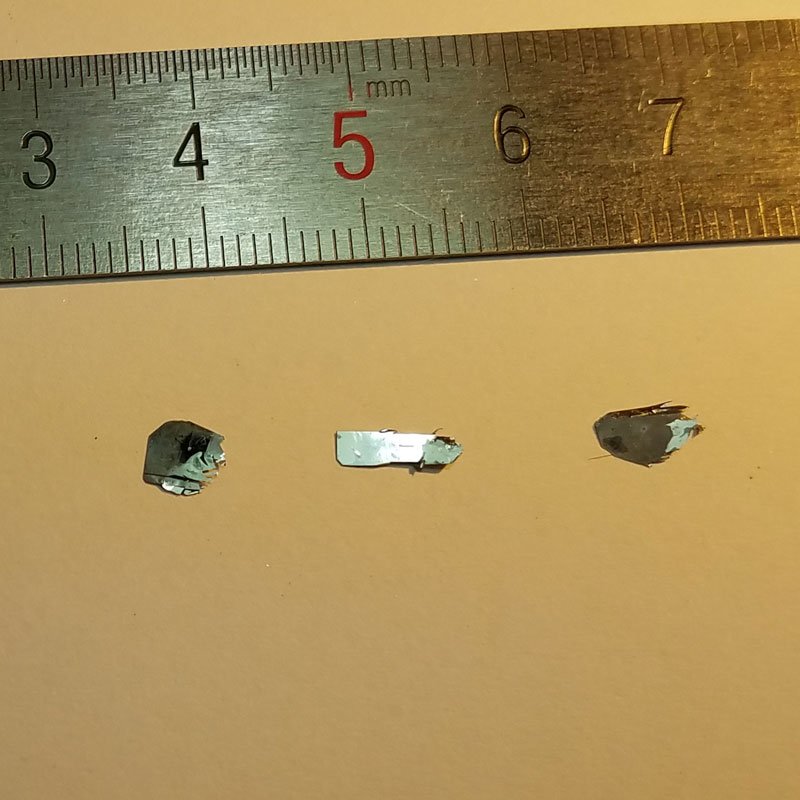
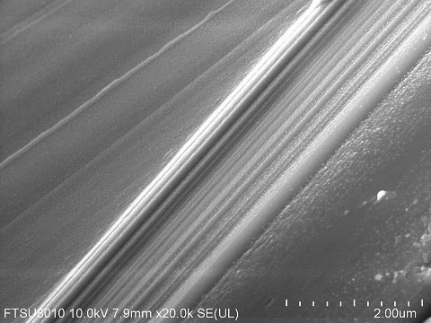
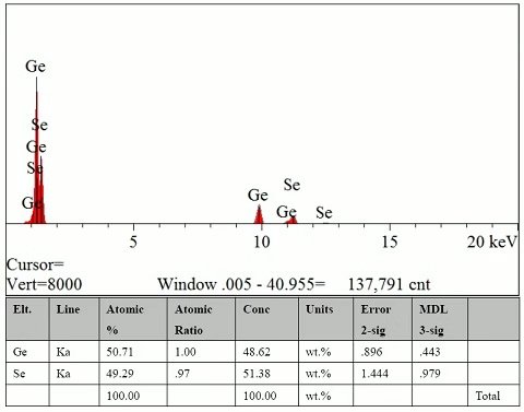
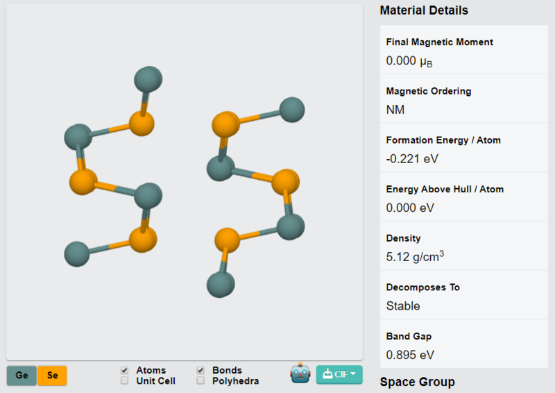
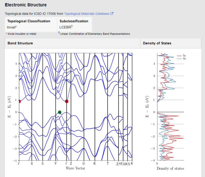
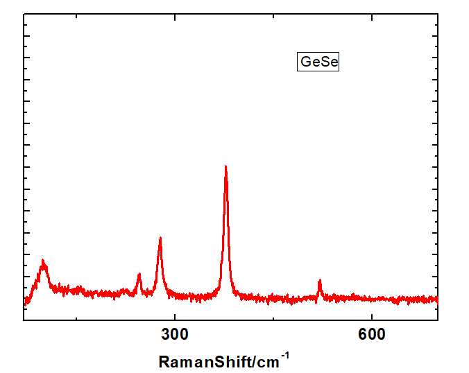
GeSe (Germanium Selenide) is a layered semiconductor material with an orthorhombic crystal structure. It is has its strong anisotropic electronic and optical properties, making it a promising candidate for applications in nanoelectronics, optoelectronics, thermoelectrics, and energy storage devices. Our GeSe crystals are synthesized using the Chemical Vapor Transport (CVT) method, with high purity, high crystallinity, and uniform structural properties.
Sample Size Options:
Crystals larger than 10 mm²
Crystals larger than 25 mm²
Crystals larger than 100 mm²
Material Properties:
Layered Orthorhombic Structure: Permits easy exfoliation into monolayers or few-layer nanosheets for 2D materials research.
Variable Bandgap: Making it applicable to optoelectronic and photovoltaic applications.
Anisotropic Transport Properties: Exhibits direction-dependent electronic and thermal conductivity, allowing for specialized device architectures.
High Carrier Mobility: Applicable to field-effect transistors (FETs) and nanoelectronic applications.
Strong Optical Absorption: High-efficiency light absorption in the visible and near-infrared range, applicable for photodetectors and solar energy conversion.
Thermal behavior: Good thermal and chemical behavior under ambient conditions.
Crystal Structure:
Type: Orthorhombic layered structure
Features: High crystallinity with uniform, defect-free layers, applicable for thin-film fabrication and nanoscale device assembly.
Degree of Exfoliation:
Ease of Use: Easily exfoliated into monolayers or few-layer nanosheets for 2D materials research and heterostructure applications.
Other Characteristics:
Thermoelectric Performance: Promising material for thermoelectric energy conversion due to its high Seebeck coefficient.
Photovoltaic Efficiency: Applicable for thin-film solar cells due to its strong optical absorption.
Flexible Electronics: Can be assembled into flexible optoelectronic and nanoelectronic devices.
Applications:
Optoelectronics:
Applicable to photodetectors, infrared sensors, and photovoltaic devices. Nanoelectronics:
Standard material for transistors, logic devices, and flexible electronics. Thermoelectric Devices:
Potential for thermoelectric energy conversion and waste heat recovery.
2D Material Studies:
Applicable for exfoliation into monolayers and assembly into van der Waals heterostructures. Energy Storage:
Potential applications in lithium-ion batteries and supercapacitors. Synthesis Method:
Chemical Vapor Transport (CVT): With quality crystals with purity, uniform thickness, and high structural integrity.
| Option 1 | > 10 mm², > 100 mm², > 25 mm² |
|---|
Related products
-
VS₂ Crystals
Price range: $883.07 through $1,006.70 -
NiI₃ Crystals
Price range: $883.07 through $1,589.54 -
FeCl₃ Crystals
Price range: $883.07 through $1,589.54 -
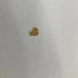
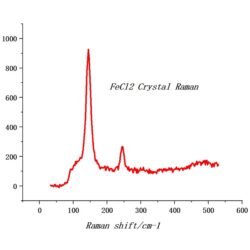
FeCl₂ Crystals
Price range: $883.07 through $1,006.70 -
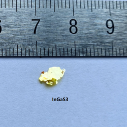
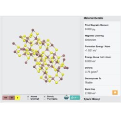
InGaS₃ Crystals
$883.07 -
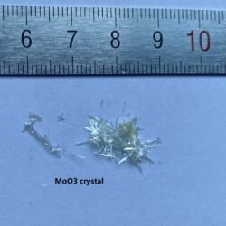
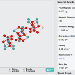
α-MoO₃ Crystals
Price range: $812.42 through $883.07 -
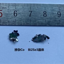
Co-Doped Bi₂Se₃ Crystals
$883.07 -
NiI₂ Crystals
Price range: $883.07 through $1,764.39 -
BiOCl Crystals
Price range: $883.07 through $1,006.70 -
VI₃ Crystals
Price range: $883.07 through $1,059.69