
BiI₃ Crystals
BiI₃ is a layered semiconductor with a van der Waals structure, investigated for its potential applications in optoelectronics, photovoltaics, and specialized 2D material research. Its indirect bandgap and high optical properties make it applicable to light-sensitive applications.
Sample Size Options:
Crystals larger than 10 mm²
Crystals larger than 25 mm²
Crystals larger than 100 mm²
Material Properties:
Layered van der Waals Structure: Applicable for exfoliation into thin layers.
Semiconducting Properties: Exhibits an indirect bandgap (~1.8 eV) applicable to optoelectronic applications.
High Optical Absorption: High-efficiency in the visible and near-infrared regions.
Environmental Sensitivity: Requires inert storage to maintain behavior.
Crystal Structure:
Type: Layered rhombohedral structure
Features: Cleavable into thin sheets for 2D material studies.
Degree of Exfoliation:
Ease of Use: Easily exfoliated into thin layers for specialized research and device applications.
Other Characteristics:
Optoelectronic Performance: High optical absorption and bandgap tunability for photonic devices.
Photovoltaic Potential: Promising material for solar cells and other energy-related technologies.
Chemical behavior: Consistent under inert conditions, applicable to long-term research.
Applications:
Optoelectronics:
Applicable for photodetectors, light sensors, and near-infrared photonic devices.
2D Material Studies:
Applicable to exfoliation into thin layers and exploration of heterostructures in van der Waals systems. Photovoltaics:
Promising for solar cell applications due to its optical and electronic properties. Quantum Materials Research:
Relevant for studying low-dimensional semiconductors and their optoelectronic behavior. Sensors:
High sensitivity to light and environmental changes, making it applicable for optical and chemical sensing.
| Option 1 | > 10 mm², > 100 mm², > 25 mm² |
|---|
Related products
-
HOPG
kr6,381.94 -
PdTe₂ Crystals
kr6,647.86 -
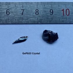
GePbS₃ Crystals
kr6,647.86 -
VI₃ Crystals
Price range: kr6,647.86 through kr7,977.46 -
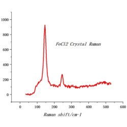
FeCl₂ Crystals
Price range: kr6,647.86 through kr7,578.58 -
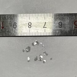
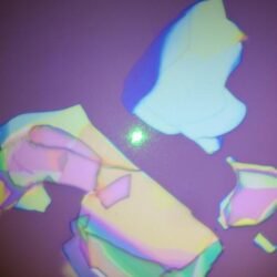
BiOCl Crystals
Price range: kr6,647.86 through kr7,578.58 -
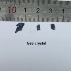
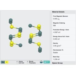
GeS Crystals
Price range: kr6,647.86 through kr7,312.66 -
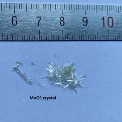
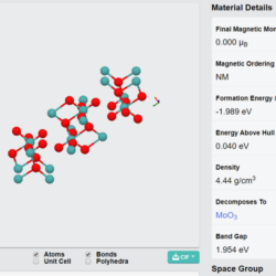
α-MoO₃ Crystals
Price range: kr6,116.02 through kr6,647.86 -
FeBr₃ Crystals
Price range: kr6,248.98 through kr6,647.86 -
InGaS₃ Crystals
kr6,647.86