
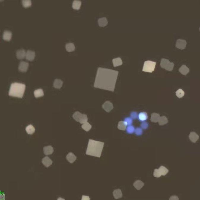
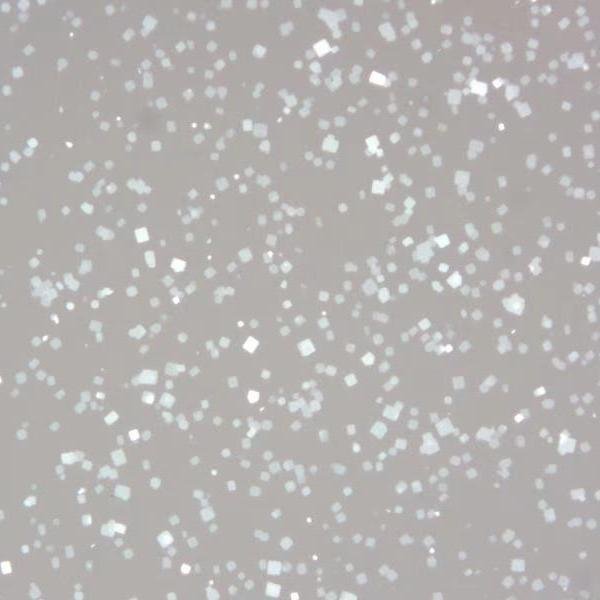
Bismuth Oxyselenide (Bi₂O₂Se)
CAS Number: N/A
Substrate Size: 1 cm x 1 cm
Preparation Method: Chemical Vapor Deposition (CVD)
Substrate Options:
Bi₂O₂Se films are directly grown on mica or sapphire substrates. Custom transfer to other substrates is available upon request-please visit the Custom Products page or contact us for assistance.
Fundamental Properties:
Bismuth oxyselenide (Bi₂O₂Se) is a layered compound with an orthorhombic crystal structure and is a two-dimensional (2D) semiconductor. Bi₂O₂Se exhibits a wide bandgap of approximately 0.8 eV in bulk form, with tunability in ultrathin layers. It has carrier mobility up to ~450 cm²/V-s at room temperature and environmental stability; these are properties of this 2D semiconductor. Bi₂O₂Se combines electrical conductivity with low thermal conductivity, and it is used in electronics, thermoelectrics, and optoelectronics. Its intrinsic stability and compatibility with scalable fabrication techniques support use in device integration.
Applications:
Electronics: Carrier mobility and stability support Bi₂O₂Se use for field-effect transistors (FETs) and other electronic devices.
Optoelectronics: Bi₂O₂Se’s semiconducting properties are used for photodetectors and light-emitting devices.
Thermoelectric Devices: Its combination of electrical and thermal properties supports its use in thermoelectric power generation and cooling applications.
Sensors: Bi₂O₂Se-based sensors exhibit sensitivity and response for gas and chemical detection.
– Energy Applications: Bi₂O₂Se is being explored for energy conversion and storage devices due to its stability and electrical properties
| オプション1 | 2 nm thin Films, 20 nm thin Films, 5 nm thin Films, Isolated Crystallites |
|---|---|
| オプション2 | Mica, Sapphire (Double-Side Polished), Sapphire (Single-Side Polished) |
関連商品
-
Bismuth Selenide (Bi₂Se₃)
¥95,593 -
-
-

-
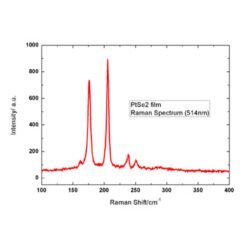
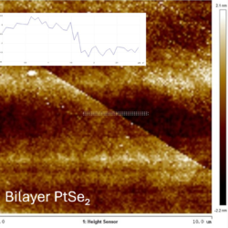
Platinum Diselenide (PtSe₂)
¥95,593 -
Tin Sulfide (SnS)
¥95,593 -

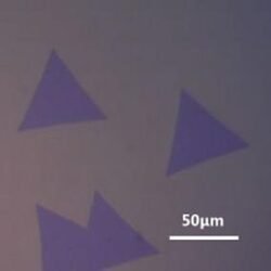
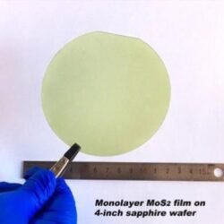
Molybdenum Disulfide (MoS₂)
元の価格は ¥93,370 でした。¥84,033現在の価格は ¥84,033 です。 Hot10% off -

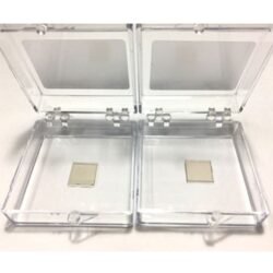
Tungsten Diselenide (WSe₂)
¥95,593 -
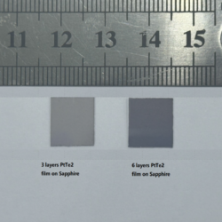
Platinum Ditelluride (PtTe₂)
¥95,593 -
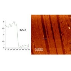
Rhenium Diselenide (ReSe₂)
¥95,593