
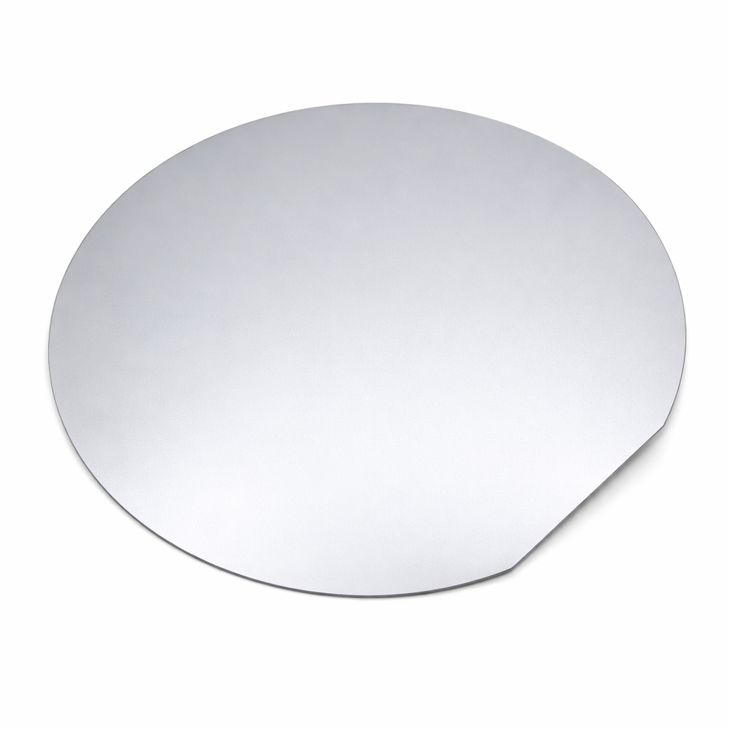
Aluminum Oxide (Al₂O₃) Thin Film on Si (100) Wafers
Price range: kr.1,708.58 through kr.2,245.33
Aluminum Oxide (Al₂O₃) Thin Film on Si (100) Wafers
Overview
Our aluminum oxide (Al₂O₃) thin film wafers are fabricated on quality Si (100) substrates to has uniform, quality dielectric and surface protection layers for research and device fabrication.
Al₂O₃ thin films has high electrical insulation, chemical behavior, good thermal resistance, and consistent surface passivation properties. These wafers are used in semiconductor research, dielectric layer studies, interface engineering, and thin film device development.
Layer Structure
Al₂O₃ (Aluminum Oxide layer)
Si (100) substrate
Recommended Film Thickness
20 nm – Most available thickness
50 nm – General dielectric applications
100 nm – Thick insulating layer
Substrate Specifications
Crystal Orientation: Si (100)
Type: N-type
Resistivity: 1–10 Ω·cm
Wafer Thickness: 500–525 µm
Surface Finish: Single-side polished (SSP)
Configuration
Single-side polished + Single-side Al₂O₃ (standard)
Double-side coating available upon request.
Film Characteristics
Good thickness uniformity
Consistent dielectric performance
High chemical resistance
Low defect density
Research-grade surface quality
Applications
High-k dielectric research
Surface passivation
MOS capacitor structures
Gate dielectric studies
Interface engineering research
Protective and barrier layer applications
Thin film device prototyping
Quality & Packaging
Clean-room fits handling
Carefully packaged to prevent contamination
Research-grade wafer quality
Custom thickness and wafer sizes available upon request.
| Option 1 | 4″ Si | 100 nm Al2O3, 4″ Si | 20 nm Al2O3, 4″ Si | 50 nm Al2O3 |
|---|
Related products
-
Aluminum Oxide (Al₂O₃) Thin Film on Si (100) Substrates (10 × 10 mm)
Price range: kr.635.07 through kr.742.42