
CuInS₂ Crystals
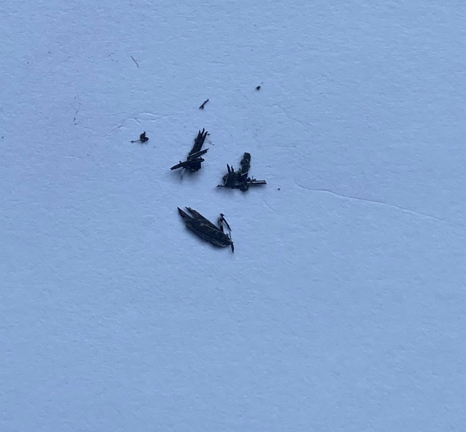
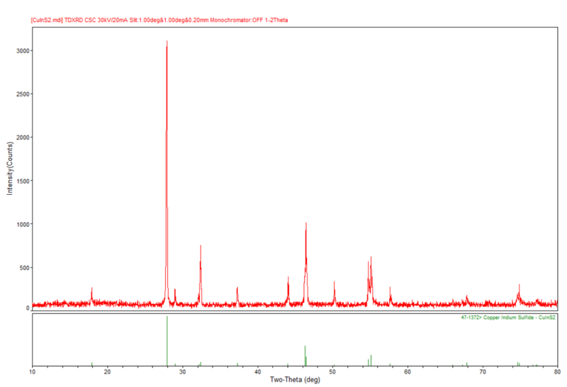
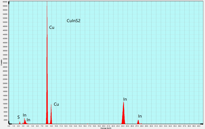
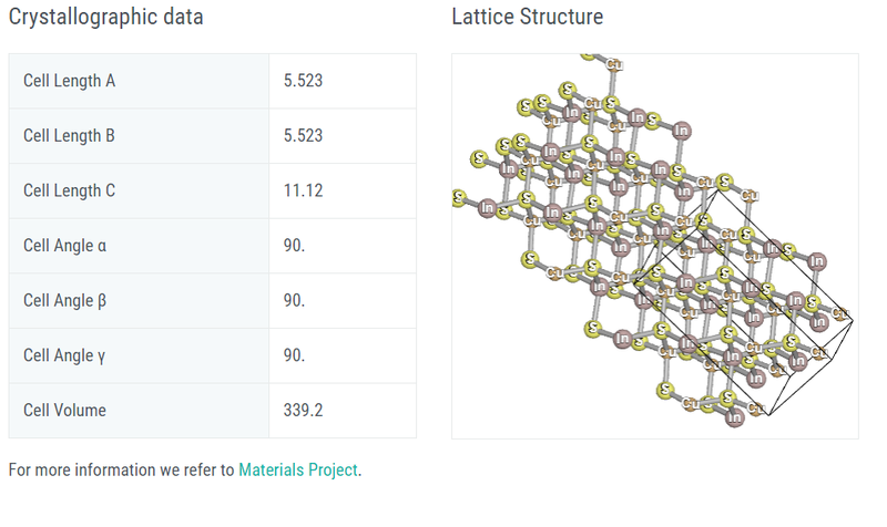
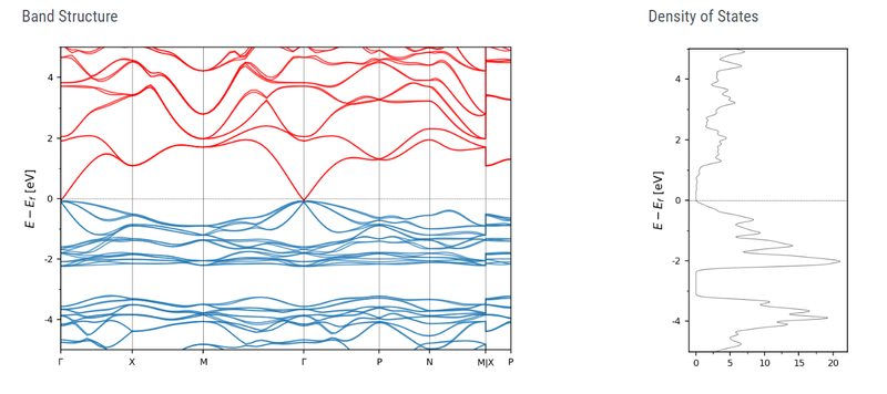
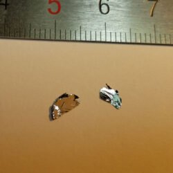
CuInS₂ is a layered chalcopyrite semiconductor has its strong optical and electronic properties. With a variable direct bandgap (~1.5 eV) and strong optical absorption, it is used in optoelectronics, photovoltaics, and specialized 2D material studies. Our CuInS₂ crystals are synthesized using high-temperature methods to with high purity, high crystallinity, and consistent performance for specialized research.
Sample Size Options: Crystals larger than 10 mm²
Crystals larger than 25 mm²
Material Properties: Semiconducting Behavior: Direct bandgap (~1.5 eV) applicable for optoelectronic applications.
High Optical Absorption: High-efficiency absorption in the visible spectrum, making it applicable to photovoltaic devices.
Layered Structure: Permits exfoliation into thin layers for nanoscale research.
Environmental behavior: Maintains properties under controlled conditions.
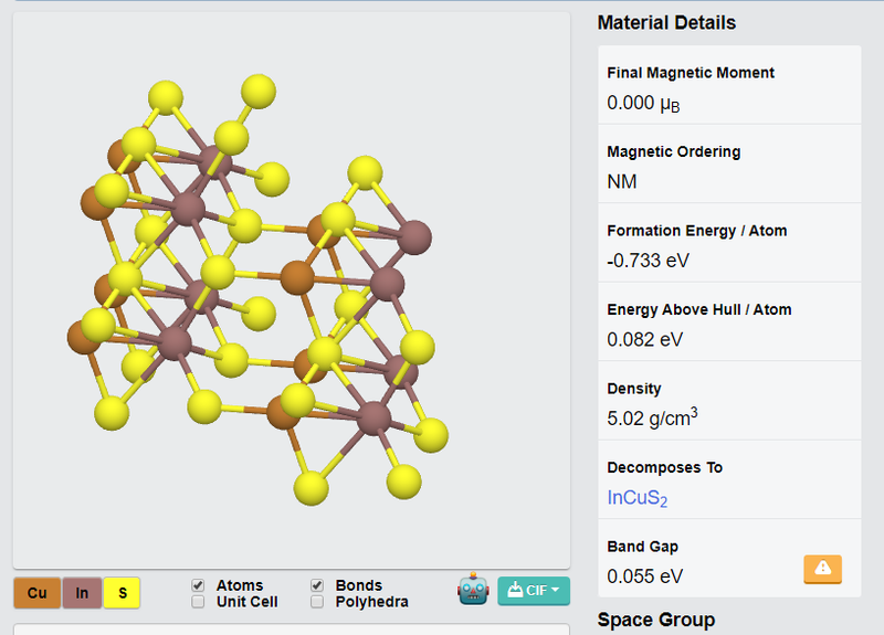
Crystal Structure: Type: Chalcopyrite layered structure
Features: Cleavable into thin sheets, applicable to 2D material studies and heterostructure fabrication.
Degree of Exfoliation: Ease of Use: Readily exfoliates into monolayers or few-layer sheets for specialized research applications.
Other Characteristics: Optoelectronic Potential: High quantum efficiency and strong photoluminescence, applicable for photodetectors and light-emitting devices. Photovoltaic
Applications: Strong light absorption and bandgap tunability make it applicable to solar cells. Energy
Applications: Promising for energy conversion and storage technologies.
Applications: Optoelectronics: Applicable to LEDs, photodetectors, and lasers.
Photovoltaics: Used in thin-film solar cells due to its high light absorption.
2D Material Studies: Applicable for exfoliation into thin layers and assembly with van der Waals heterostructures.
Quantum Materials Research: Permits studies of low-dimensional semiconducting and optoelectronic properties. Energy
Applications: Promising for photocatalysis and energy storage devices.
| Option 1 | > 10 mm², > 25 mm² |
|---|
Related products
-
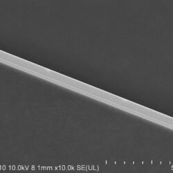
MoTe₂ Crystals (2H phase)
Price range: $968.82 through $1,104.45 -
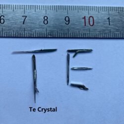
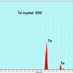
Te Crystals
$968.82 -
VS₂ Crystals
Price range: $968.82 through $1,104.45 -
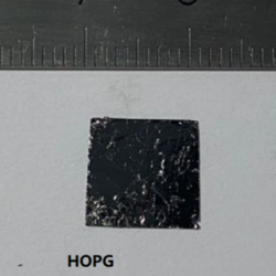
HOPG
$930.06 -
FeCl₃ Crystals
Price range: $968.82 through $1,743.89 -
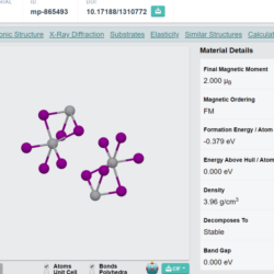
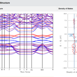
VI₃ Crystals
Price range: $968.82 through $1,162.58 -
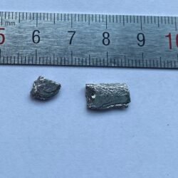
Ni₂Bi₂Te₅ Crystals
Price range: $968.82 through $1,104.45 -
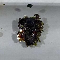
CrBr₃ Crystals
$968.82 -
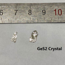
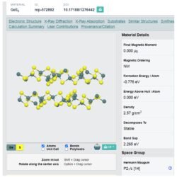
GeS₂ Crystals
Price range: $968.82 through $1,162.58 -
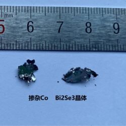
Co-Doped Bi₂Se₃ Crystals
$968.82