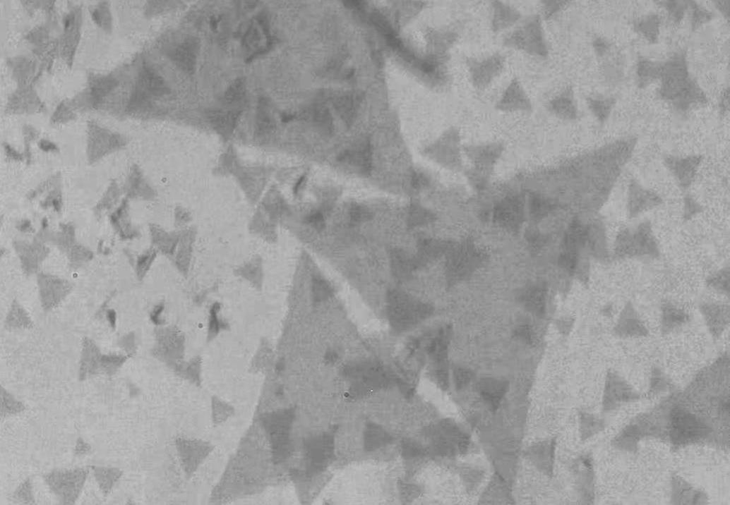
Homojunction fabrication in 2D materials involves the sequential transfer of identical 2D materials, creating a layered structure with the same material. This process is particularly useful for applications that require enhanced material properties, such as increased active surface area or improved electronic coupling. In our wet transfer method, clients can choose the same 2D material, such as MoS₂, to fabricate a homojunction.
For example, the process could involve transferring a larger MoS₂ layer, followed by a smaller MoS₂ layer (as illustrated in the image). This technique uses a PMMA-assisted wet transfer approach to ensure smooth and accurate transfers onto a variety of substrates, such as PET, PI, ITO, FTO, glass, metals, etc.
Homojunctions have applications in electronic devices, optoelectronics, and catalysis, where uniform material composition is essential for consistent performance. This fabrication process allows for the precise layering of identical materials, enabling the exploration of novel device architectures and enhanced functionalities in 2D material systems.
Our wet transfer service for homojunction fabrication offers flexibility and control, allowing clients to integrate homojunctions onto their preferred substrates and take advantage of the unique properties that come with layered 2D materials.