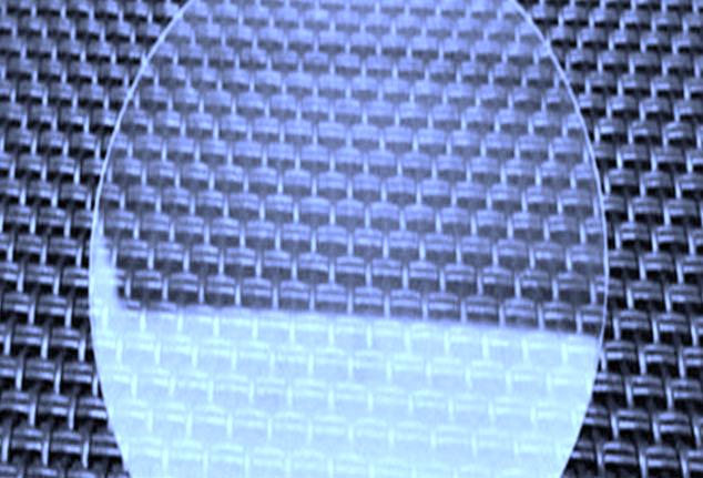
Our wafer thinning and polishing services ensure precise material reduction and surface refinement, essential for high-performance MEMS and semiconductor applications. Thinning removes excess material from the wafer’s backside, achieving the desired thickness for efficient packaging, while polishing reduces surface roughness to create a smooth, reflective finish.
Thinning: Compatible with materials such as silicon (Si), gallium arsenide (GaAs), gallium nitride (GaN), indium phosphide (InP), glass, sapphire, and ceramics. Our process achieves uniformity within ±2 μm across the wafer surface.
Polishing: Available for Si, GaAs, GaN, InP, glass, sapphire, and ceramic substrates, achieving surface roughness levels from 1 to 50 nm, essential for applications requiring high surface quality and optical clarity.
