
Description
Tin Sulfide (SnS)
CAS Number: 1314-95-0
Substrate Size: 1 cm × 1 cm
Preparation Method: Chemical Vapor Deposition (CVD)
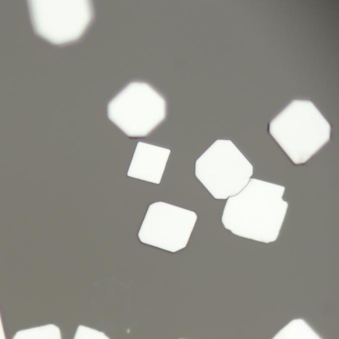
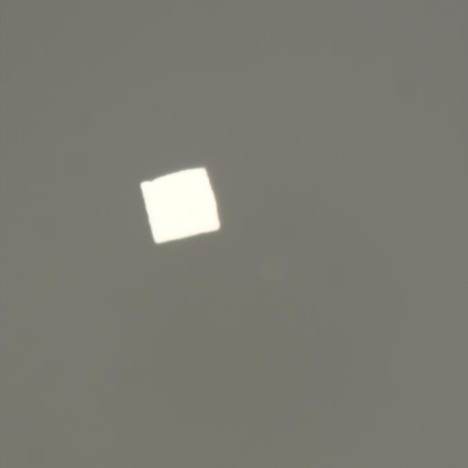
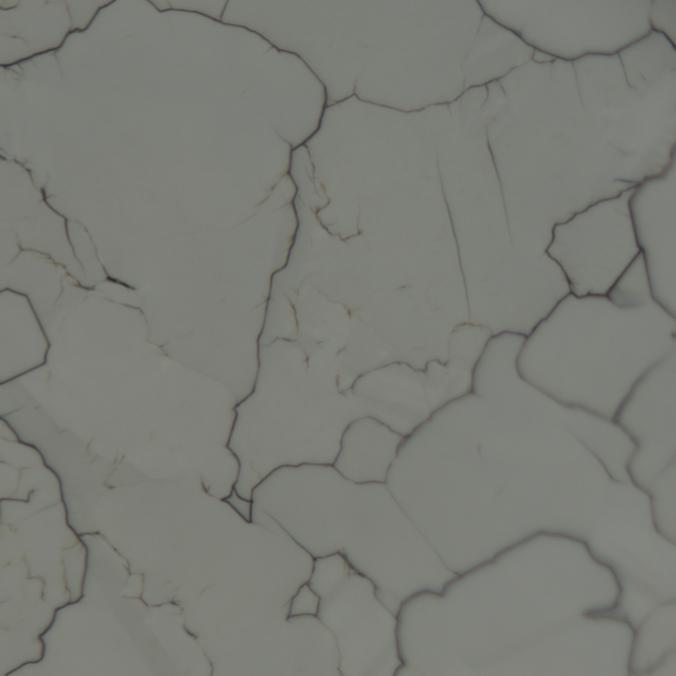
Morphology Options:
Isolated Crystallites
Continuous Multilayer Film
For specific requirements regarding morphology or thickness, please contact us directly.
Substrate Options:
SnS films are directly grown on sapphire substrates. Custom transfer to other substrates is available upon request—please visit our Custom Products page or contact us for assistance.
Fundamental Properties:
Tin sulfide (SnS) is a layered material with an orthorhombic crystal structure and is a promising p-type semiconductor. It has a direct bandgap of approximately 1.3 eV in monolayer form and an indirect bandgap of about 1.1 eV in bulk, making it suitable for optoelectronic and photovoltaic applications.
SnS is known for its high absorption coefficient, environmental stability, and abundance, making it an eco-friendly and cost-effective material for energy-related applications. Its layered structure facilitates integration into nanoscale devices.
Applications:
Optoelectronics: The direct bandgap of SnS makes it ideal for photodetectors, LEDs, and solar cells.
Electronics: SnS is suitable for field-effect transistors (FETs) and other thin-film electronic devices due to its semiconducting properties.
Sensors: SnS-based devices demonstrate excellent sensitivity for gas and chemical sensing.
Energy Applications: SnS is widely studied for its potential in solar cells and as an electrode material in batteries and supercapacitors.
Photocatalysis: The optical properties of SnS enable its use in photocatalytic applications, including water splitting.
Additional information
| CAS Number |
|---|