Description
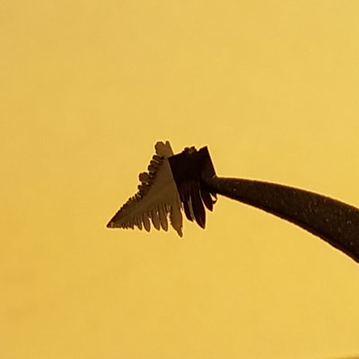
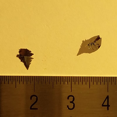
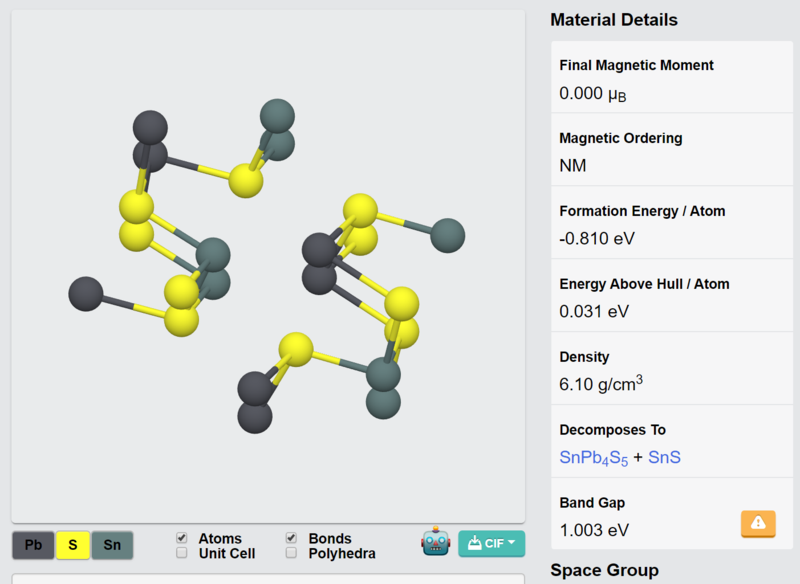
PbSnS₂ Crystals (Lead Tin Disulfide)
PbSnS₂ is a layered ternary chalcogenide material with excellent thermoelectric, electronic, and optoelectronic properties. Its tunable bandgap, high carrier mobility, and strong light absorption make it a promising candidate for energy conversion, photodetectors, and 2D material studies.
Sample Size Options:
Crystals larger than 10 mm²
Crystals larger than 25 mm²
Crystals larger than 100 mm²
Material Properties:
Layered Structure: Facilitates exfoliation into thin layers for 2D material research.
Tunable Bandgap: Suitable for optoelectronic and photonic applications.
Thermoelectric Efficiency: High potential for energy harvesting and cooling technologies.
Optical Absorption: Strong absorption in the visible and infrared ranges.
Crystal Structure:
Type: Layered structure with van der Waals interactions
Features: Cleavable layers ideal for thin-film fabrication and nanoscale device research.
Degree of Exfoliation:
Ease of Use: Readily exfoliates into thin layers for advanced research and applications.
Other Characteristics:
Thermoelectric Applications: High performance for waste heat recovery and energy conversion.
Optoelectronic Potential: Excellent photoluminescence and optical properties for cutting-edge devices.
Quantum Research Opportunities: Enables exploration of electronic transport and quantum phenomena in layered chalcogenides.
Applications:
Optoelectronics:
Ideal for photodetectors, light sensors, and advanced photonic devices.
Thermoelectric Devices:
Promising for waste heat recovery and energy harvesting systems.
Energy Applications:
Suitable for catalytic processes and energy storage solutions.
2D Material Studies:
Perfect for exfoliation into monolayers and integration into van der Waals heterostructures.
Sensors:
High sensitivity for detecting environmental and chemical stimuli.
Additional information
| CAS Number | N/A |
|---|