
Description
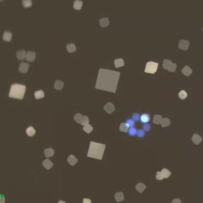
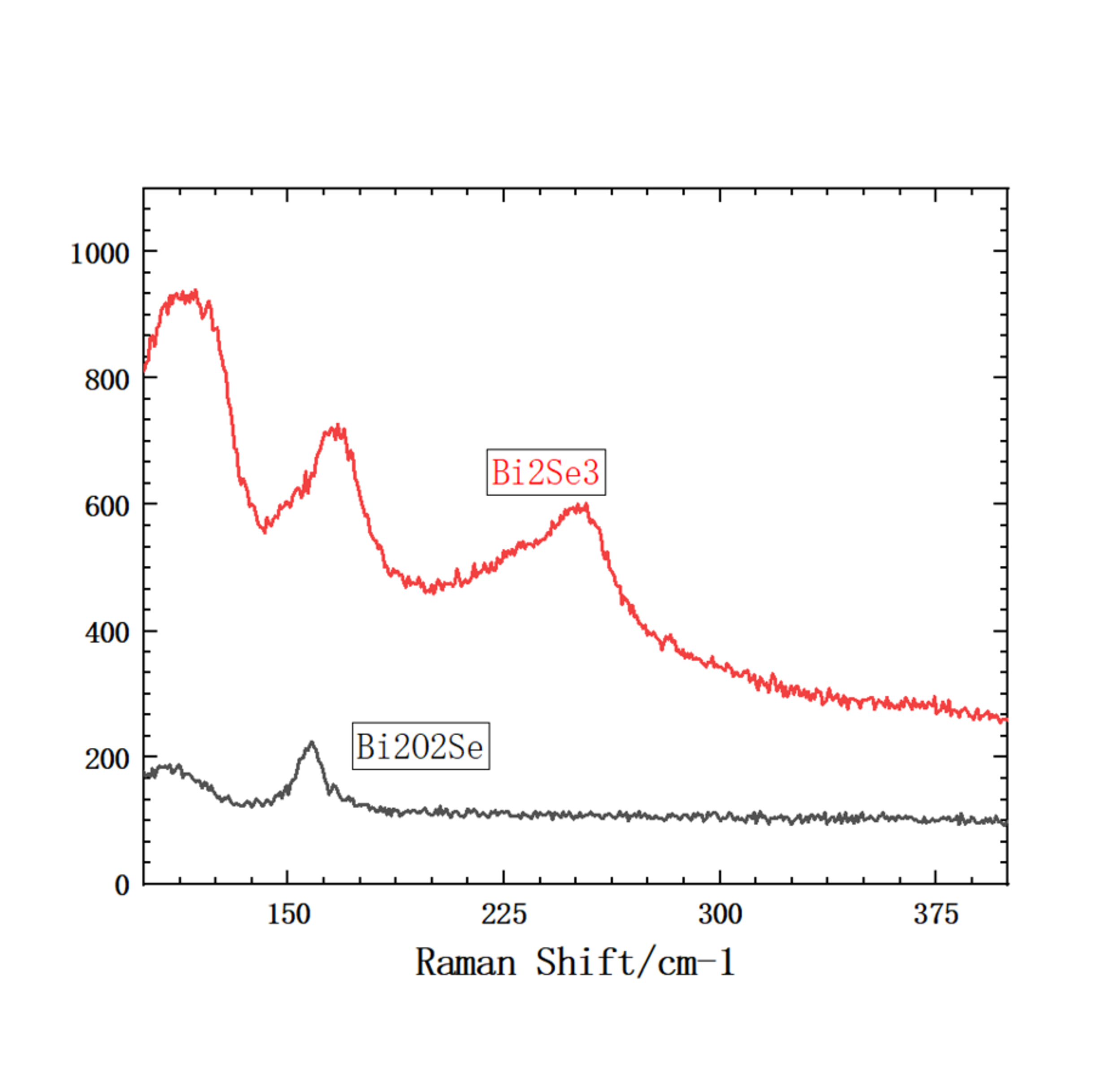
Bismuth Oxyselenide (Bi₂O₂Se)
CAS Number: N/A
Substrate Size: 1 cm × 1 cm
Preparation Method: Chemical Vapor Deposition (CVD)
Substrate Options:
Bi₂O₂Se films are directly grown on mica or sapphire substrates. Custom transfer to other substrates is available upon request—please visit our Custom Products page or contact us for assistance.
Fundamental Properties:
Bismuth oxyselenide (Bi₂O₂Se) is a layered compound with an orthorhombic crystal structure and is considered a promising two-dimensional (2D) semiconductor. Bi₂O₂Se exhibits a wide bandgap of approximately 0.8 eV in bulk form, with potential for tuning in ultrathin layers. It is well-known for its excellent carrier mobility (up to ~450 cm²/V·s at room temperature) and environmental stability, distinguishing it from many other 2D semiconductors.
Bi₂O₂Se combines high electrical conductivity with low thermal conductivity, making it suitable for applications in electronics, thermoelectrics, and optoelectronics. Its intrinsic stability and compatibility with scalable fabrication techniques make it a promising material for practical device integration.
Applications:
Electronics: High carrier mobility and stability make Bi₂O₂Se an ideal material for field-effect transistors (FETs) and other electronic devices.
Optoelectronics: Bi₂O₂Se’s semiconducting properties are suitable for photodetectors and light-emitting devices.
Thermoelectric Devices: Its combination of electrical and thermal properties enables its use in thermoelectric power generation and cooling applications.
Sensors: Bi₂O₂Se-based sensors exhibit high sensitivity and reliability for gas and chemical detection.
• Energy Applications: Bi₂O₂Se is being explored for energy conversion and storage devices due to its stability and unique electrical properties
Additional information
| CAS Number |
|---|