Description
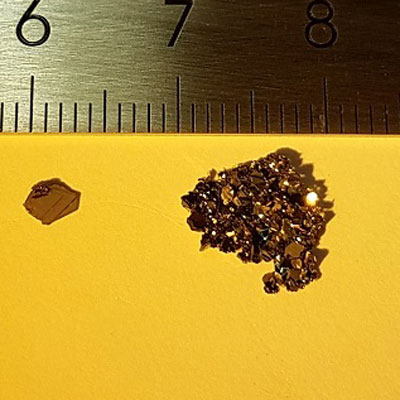
BiSe Crystals (Bismuth Selenide)
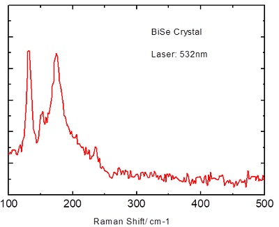
BiSe is a layered material with a van der Waals structure, exhibiting excellent thermoelectric and optoelectronic properties. Its unique electronic structure and high environmental stability make it a promising candidate for thermoelectric devices, quantum material research, and advanced optoelectronic applications.
Sample Size Options:
Crystals larger than 10 mm²
Crystals larger than 25 mm²
Crystals larger than 100 mm²
Material Properties:
Layered Van der Waals Structure: Facilitates exfoliation into thin layers for 2D material studies.
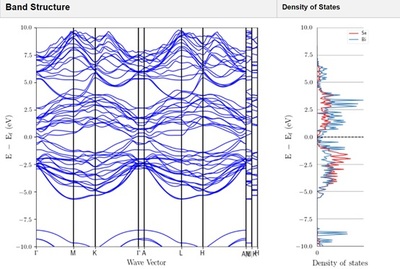
Semiconducting Behavior: Moderate bandgap ideal for electronic and photonic applications.
Thermoelectric Potential: Exhibits a high Seebeck coefficient and low thermal conductivity for energy conversion.
Optical Absorption: Strong absorption in the visible to near-infrared range.
Crystal Structure:
Type: Hexagonal layered structure
Features: Easily cleavable layers suitable for thin-film fabrication and nanoscale research.
Degree of Exfoliation:
Ease of Use: Readily exfoliates into monolayers or few-layer sheets for advanced material studies.
Other Characteristics:
Thermoelectric Efficiency: High performance for energy harvesting and cooling devices.
Quantum Research Potential: Enables exploration of quantum confinement and topological phenomena.
Optoelectronic Properties: Strong photoluminescence and high carrier mobility for advanced devices.
Applications:
Thermoelectric Devices:
Ideal for power generation, cooling systems, and waste heat recovery.
Optoelectronics:
Suitable for photodetectors, light sensors, and advanced photonic devices.
Quantum Materials Research:
Promising for studying topological states and electronic transport phenomena.
2D Material Studies:
Perfect for exfoliation into thin layers and integration into van der Waals heterostructures.
Sensors:
High sensitivity for environmental and chemical sensing applications.
Additional information
| CAS Number | N/A |
|---|