Description
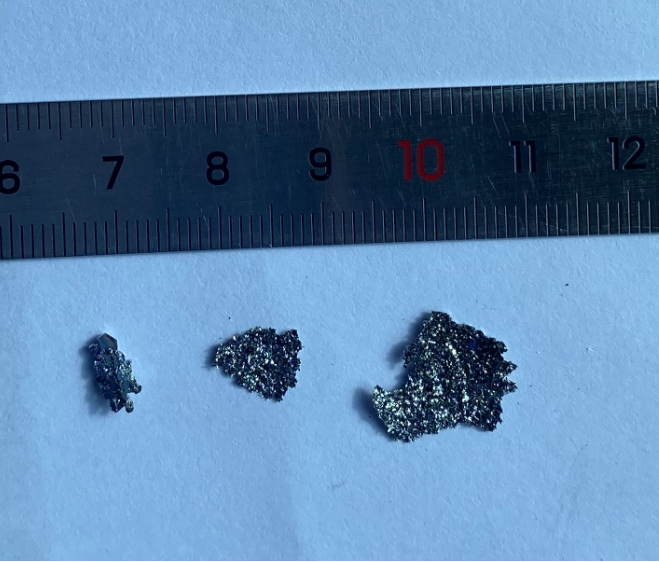
Bi₄Pb₇Se₁₃ Crystals (Bismuth Lead Selenide)
Bi₄Pb₇Se₁₃ is a layered thermoelectric material with a van der Waals structure, combining exceptional electronic, optical, and thermoelectric properties. Its high thermoelectric efficiency, strong spin-orbit coupling, and structural stability make it a promising material for quantum materials research, energy harvesting, and spintronics. Our Bi₄Pb₇Se₁₃ crystals are synthesized using the Chemical Vapor Transport (CVT) method, ensuring high purity, precise stoichiometry, and superior crystallinity.
Sample Size Options:
Crystals larger than 10 mm²
Crystals larger than 25 mm²
Crystals larger than 100 mm²
Material Properties:
Layered Van der Waals Structure: Facilitates exfoliation into thin layers for 2D material studies.
Thermoelectric Efficiency: High Seebeck coefficient and low thermal conductivity for energy harvesting applications.
Electronic Conductivity: Excellent carrier mobility for electronic and thermoelectric devices.
Optical Absorption: Strong absorption in the visible-to-infrared range, ideal for photonic devices.
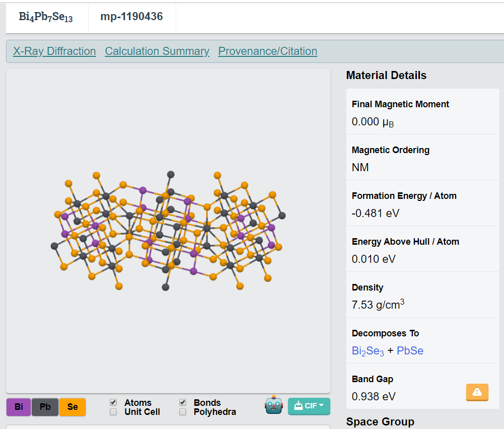
Crystal Structure:
Type: Rhombohedral layered structure
Features: Cleavable layers, suitable for thin-film fabrication and nanoscale device integration.
Degree of Exfoliation:
Ease of Use: Readily exfoliates into monolayers or few-layer sheets for advanced research.
Other Characteristics:
Quantum Properties: Promising for studying topological surface states and quantum transport phenomena.
Thermoelectric Applications: Ideal for energy harvesting and thermal management systems.
Spintronics Applications: Suitable for exploring spin-based devices and spin-orbit coupling.
Applications:
Quantum Materials Research:
Enables exploration of topological insulators and associated quantum phenomena.
Thermoelectric Devices:
Promising for energy conversion and cooling technologies.
Spintronics:
Ideal for spin-based devices and spintronic memory technologies.
2D Material Studies:
Perfect for exfoliation into thin layers and integration into van der Waals heterostructures.
Optoelectronics:
Suitable for photodetectors, sensors, and other optoelectronic devices.
Additional information
| CAS Number | N/A |
|---|