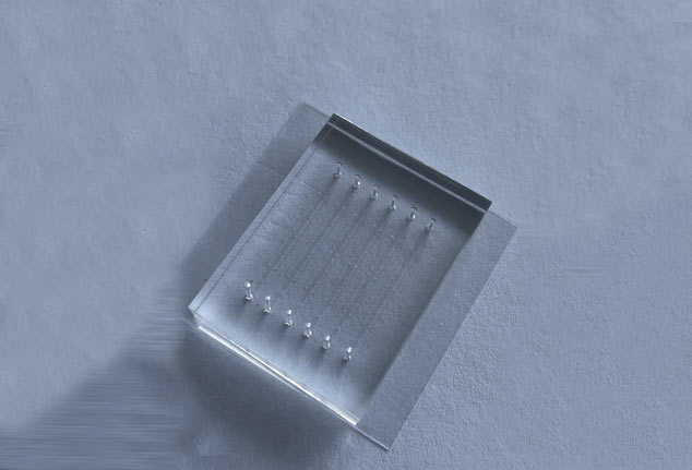
Our microfluidic device fabrication services utilize advanced lithography techniques from the microelectronics industry, combined with soft lithography for surface patterning, to create precise microchannel structures. To form fully functional microfluidic channels, we employ bonding techniques tailored to the materials used, including high-temperature, high-pressure, or high-voltage bonding for glass and silicon, and oxygen plasma bonding for PDMS materials.
PDMS Devices: Fabricated with high-precision molds, offering micron-level line widths for reliable, flexible microchannel applications.
Silicon Microchannels: Achieving nano-level line widths with controllable precision within ±5%, and an aspect ratio of up to 20:1, ideal for high-aspect-ratio microstructures.
Glass Microchannels: Designed with micron-level depth and precision control within ±10%, supporting an aspect ratio of up to 1:2 for robust glass microfluidic systems.