MEMS FABRICATION

Explore your design ideas with our engineers, we create products based on your designs.

Home > MEMS Fabrication

Photolithography

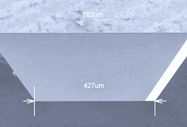
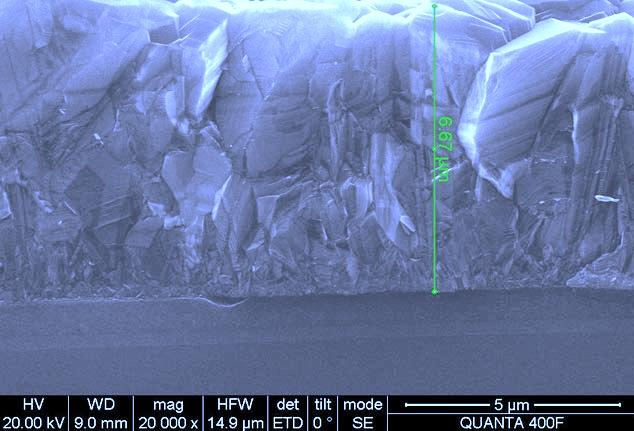
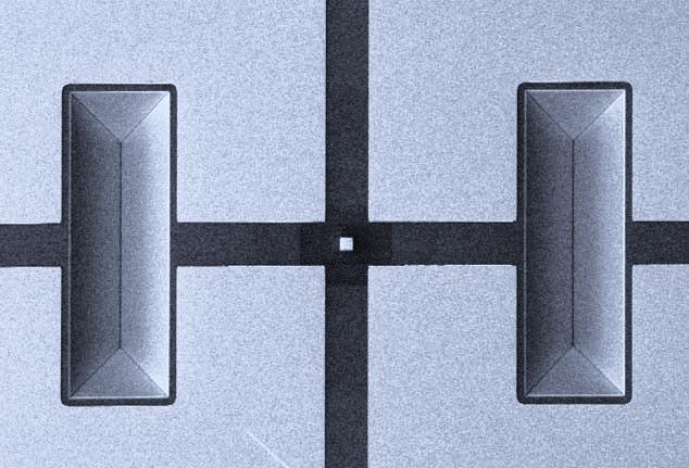
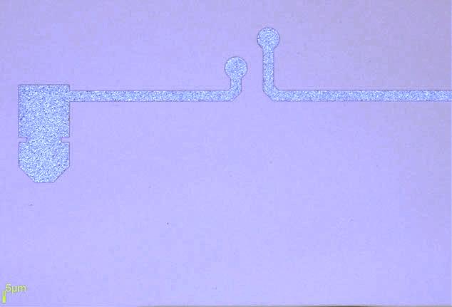
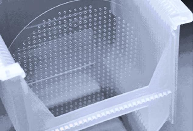
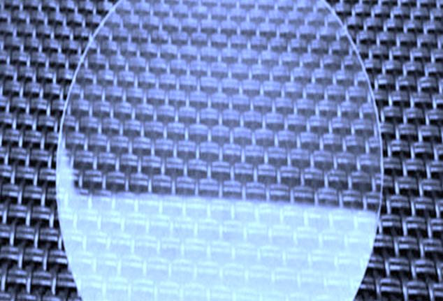
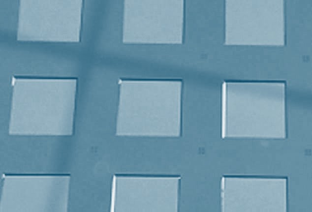
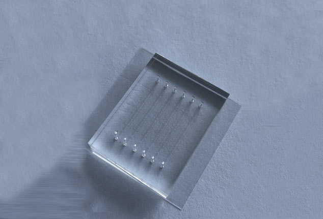
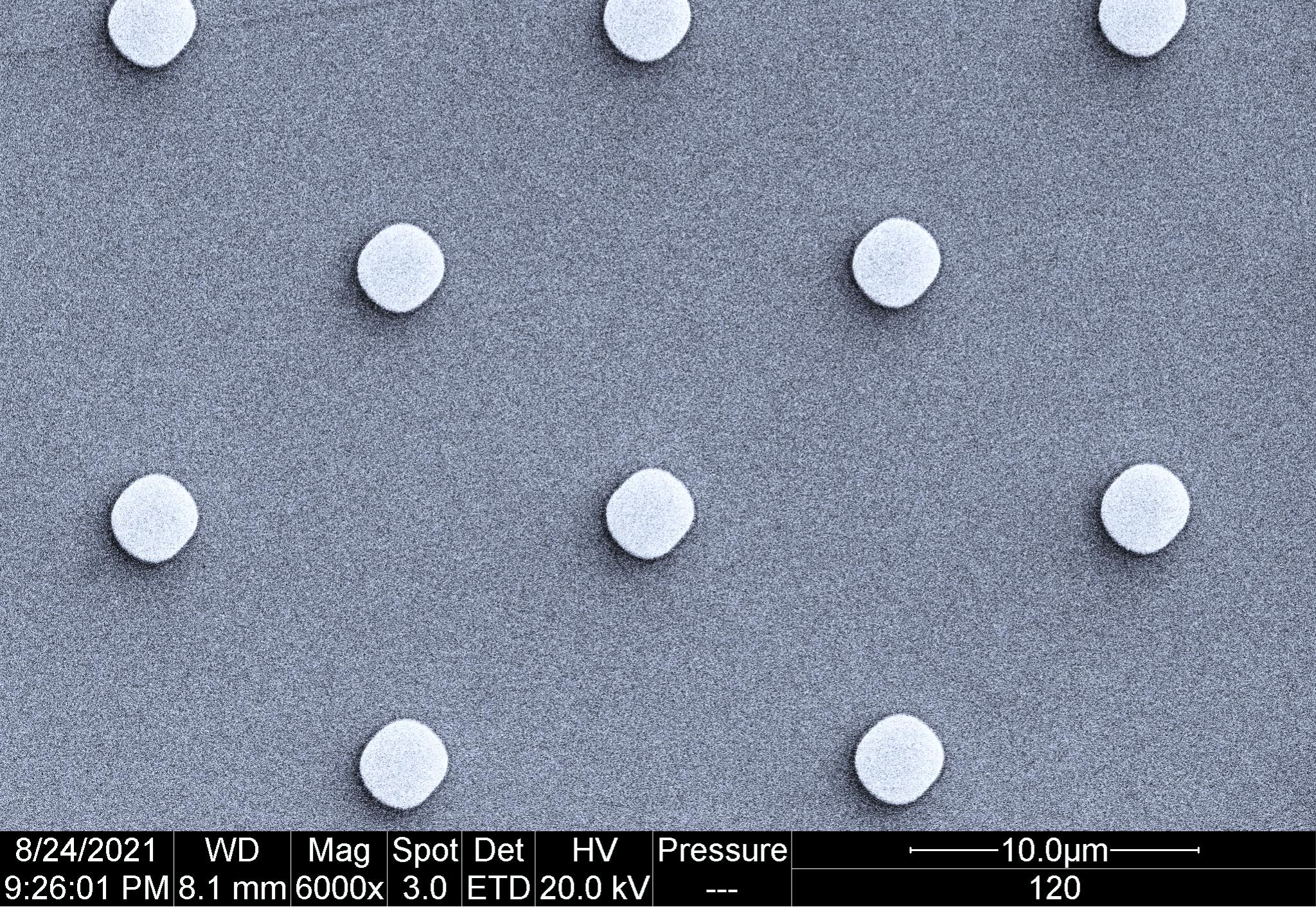
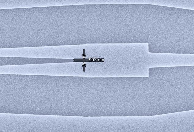
Photolithography is a cornerstone of semiconductor and MEMS fabrication, enabling precise patterning at the microscale and nanoscale. This advanced technique uses light to transfer intricate patterns onto wafer surfaces, creating openings in masking layers like silicon dioxide for localized impurity diffusion. Essential for defining device structures, photolithography allows for high-resolution patterning, layer alignment, and miniaturization, which are crucial for producing complex integrated circuits and MEMS devices. With state-of-the-art photolithography processes, we support innovations in electronics, sensors, and nanotechnology, providing the precision and control needed for next-generation device manufacturing. Applicable Substrates: Silicon wafers, glass, sapphire, flexible materials, and other substrates. Contact Lithography: Minimum feature size: 1 μm; overlay accuracy: ±0.5 μm. Stepper Projection Lithography: Projection ratio: 1:5; minimum feature size: 0.35 μm; overlay accuracy: ≤0.15 μm (X, Y); maximum exposure field: <22 x 22 mm. Electron Beam Lithography (EBL): Minimum feature size: 10 nm; overlay accuracy: 40 nm; maximum exposure diameter: <100 mm. Double-Sided Lithography: Minimum feature size: 1 μm; front-side overlay accuracy: ±1 μm; backside overlay accuracy: ±2 μm.

Etching

Etching is a critical process in MEMS fabrication, allowing for precise patterning and material removal across a range of substrates and material types. Our advanced etching capabilities include both chemical and physical methods to meet diverse application needs. We offer alkaline etching with KOH and TMAH, as well as acidic etching using HF, BOE, HCl, and HNO₃, providing flexibility for various material requirements, including silicon, silicon dioxide, silicon nitride, metals, and quartz. Ion Beam Etching (IBE): Ideal for etching hard-to-remove metals and other challenging materials. Deep Reactive Ion Etching (DRIE): Ensures uniformity <±5% and offers selectivity ratios exceeding 50:1, suitable for high-aspect-ratio silicon etching. Reactive Ion Etching (RIE): Effective for etching silicon (Si), silicon dioxide (SiO₂), and silicon nitride (SiNx) with precise control. Focused Ion Beam Etching (FIB): Enables micro- and nanoscale etching, deposition, and doping of materials and devices. Inductively Coupled Plasma (ICP) Etching: Specialized for etching compound semiconductors, including GaN, GaAs, and InP.

Coating

Our MEMS thin-film deposition services offer high-quality coatings tailored for advanced applications in microelectronics, optoelectronics, and sensor technology. We provide a wide selection of both metallic and non-metallic materials, with deposition methods optimized for precision and consistency across various substrates. Deposition Materials: Metals: Ti, Al, Ni, Au, Ag, Cr, Pt, Cu, TiW (90), Pd, Zn, Mo, W, Ta, Nb, and more. Non-metals: Si, SiO₂, SiNx, Al₂O₃, HfO₂, MgF₂, ITO, Ta₂O₅, among others. Substrate Compatibility: Silicon wafers, quartz glass, sapphire, PET, PI, and other substrates. Electron Beam Evaporation: For high-purity thin films with excellent control over thickness and uniformity. Magnetron Sputtering: Ideal for uniform coatings with strong adhesion across complex surfaces. Low-Pressure Chemical Vapor Deposition (LPCVD): Ensures high-quality thin films with precise layer control. Plasma-Enhanced Chemical Vapor Deposition (PECVD): Enables low-temperature deposition for thermally sensitive materials. Atomic Layer Deposition (ALD): Provides ultra-thin, conformal coatings with atomic-level precision.

Wafer Bonding

Wafer bonding is a high-precision process that unites two meticulously cleaned, atomically smooth surfaces of either identical or different semiconductor materials. Through careful surface preparation and activation, wafers are bonded under controlled conditions using van der Waals forces, molecular interactions, or atomic bonding, resulting in a seamless, unified structure. We offer a range of advanced bonding techniques to support diverse materials and application needs. Anodic Bonding: Ideal for creating strong, hermetic seals between silicon and glass, metal and glass, semiconductor and alloy, or semiconductor and glass interfaces—crucial for high-reliability applications. Eutectic Bonding: Suitable for low-melting-point bonding with materials like PbSn, AuSn, CuSn, and AuSi, delivering superior mechanical and electrical properties for MEMS and semiconductor devices. Adhesive Bonding: Utilizing specialized adhesives such as AZ4620 and SU8, this flexible bonding solution is compatible with 4-inch and 6-inch wafers, supporting a range of materials and device types.

Epitaxy, Doping

Our epitaxy and doping services provide precise control over material properties, essential for optimizing MEMS devices and semiconductor applications. Through advanced epitaxial growth and controlled doping techniques, we offer flexible solutions tailored to a wide range of materials and applications. Metal-Organic Chemical Vapor Deposition (MOCVD): Enables the growth of high-quality epitaxial layers, ideal for materials like GaN and GaAs in optoelectronic and high-frequency applications. Chemical Vapor Deposition (CVD): Supports epitaxial growth for materials such as SiC, suitable for high-power and high-temperature devices. Ion Implantation: Provides precise doping capabilities for elements including boron (B), phosphorus (P), fluorine (F), aluminum (Al), nitrogen (N), argon (Ar), hydrogen (H), helium (He), and silicon (Si), allowing for customized electrical properties in semiconductor layers. Additional high-temperature processes, such as Thermal Oxidation, High-Temperature Diffusion/Annealing, and Rapid Thermal Annealing (RTA), further enhance material performance and reliability.

Dicing, Drilling

Our MEMS dicing and drilling services provide precise material separation and micro-hole fabrication for a wide range of applications, from semiconductor and LED chip manufacturing to medical and consumer electronics. Using advanced dicing and drilling techniques, we ensure accuracy and reliability for various substrate types and device requirements. Laser Dicing: Ideal for silicon substrates with thicknesses ranging from 100 to 700 μm; compatible with 2-inch, 4-inch, 6-inch, and 8-inch wafers. Blade Dicing: Suitable for cutting materials such as silicon (Si), germanium (Ge), glass, quartz, ceramics, and printed circuit boards, using both soft and hard blades for optimized precision. Micro-Drilling: Supports drilling micro-scale holes in various materials, essential for industries including LEDs, touchscreens, LCDs, consumer electronics, MEMS, lighting, and medical devices.

Thinning, Polishing

Our wafer thinning and polishing services ensure precise material reduction and surface refinement, essential for high-performance MEMS and semiconductor applications. Thinning removes excess material from the wafer’s backside, achieving the desired thickness for efficient packaging, while polishing reduces surface roughness to create a smooth, reflective finish. Thinning: Compatible with materials such as silicon (Si), gallium arsenide (GaAs), gallium nitride (GaN), indium phosphide (InP), glass, sapphire, and ceramics. Our process achieves uniformity within ±2 μm across the wafer surface. Polishing: Available for Si, GaAs, GaN, InP, glass, sapphire, and ceramic substrates, achieving surface roughness levels from 1 to 50 nm, essential for applications requiring high surface quality and optical clarity.

Silicon Nitride Windows

Custom silicon nitride (Si₃N₄) windows are ideal carriers for structural analysis and transmission imaging in synchrotron X-ray, soft X-ray, UV, and extreme UV applications. These thin-film windows provide exceptional thermal stability, enabling quasi-in-situ studies of sample morphology before and after annealing processes. Applications and Benefits: Versatile Sample Support: Suitable for TEM observation of materials and biological specimens, silicon nitride windows offer a high-contrast, non-toxic substrate ideal for biological sample culture and imaging. • Enhanced Analysis for Carbon-Based Samples: Silicon nitride windows minimize interference, making them excellent for EDX/EELS analysis of carbon-containing samples.

Microfluidic Devices

Our microfluidic device fabrication services utilize advanced lithography techniques from the microelectronics industry, combined with soft lithography for surface patterning, to create precise microchannel structures. To form fully functional microfluidic channels, we employ bonding techniques tailored to the materials used, including high-temperature, high-pressure, or high-voltage bonding for glass and silicon, and oxygen plasma bonding for PDMS materials. PDMS Devices: Fabricated with high-precision molds, offering micron-level line widths for reliable, flexible microchannel applications. Silicon Microchannels: Achieving nano-level line widths with controllable precision within ±5%, and an aspect ratio of up to 20:1, ideal for high-aspect-ratio microstructures. Glass Microchannels: Designed with micron-level depth and precision control within ±10%, supporting an aspect ratio of up to 1:2 for robust glass microfluidic systems.