Choose your ideal 2D material and preferred substrate.
Home > 2D Semiconctors > Mechanical Exfoliation of Monolayer /Multilayer 2D Materials
Mechanical Exfoliation of Monolayer /Multilayer 2D Materials
DESCRIPTION
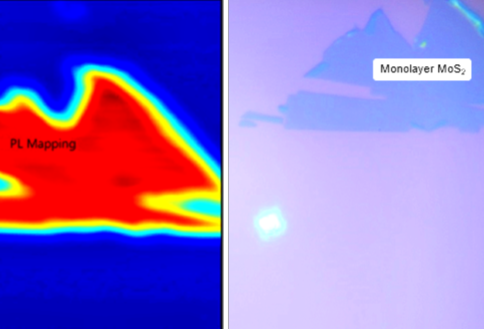
Mechanical exfoliation is a widely used method for obtaining high-quality monolayer or multilayer 2D materials directly from bulk crystals. Unlike chemical vapor deposition (CVD) or wet transfer techniques, this approach relies on the physical peeling of crystalline materials using adhesive tape, such as scotch tape, to isolate thin layers of the desired 2D material.
In this process, a bulk crystal (e.g., MoS₂, WS₂, or graphene) is carefully peeled using the tape, and the exfoliated material is then transferred onto the client’s selected substrate. This method is effective for producing pristine monolayer or multilayer regions and offers high crystallinity, making it ideal for fundamental research and device prototyping.
We provide mechanical exfoliation services on a wide range of substrates, such as PET, PI, ITO, FTO, glass, metals, and others, allowing researchers to integrate 2D materials into flexible, transparent, or conductive devices. This technique is particularly valued for applications in nanoscale electronics, photonics, and catalysis, where the intrinsic properties of the 2D material need to be preserved.
Mechanical exfoliation enables clients to access high-quality 2D material samples tailored to their specific substrate needs, ensuring they can explore novel properties and applications in their research or product development.