Etching is a critical process in MEMS fabrication, allowing for precise patterning and material removal across a range of substrates and material types. Our advanced etching capabilities include both chemical and physical methods to meet diverse application needs. We offer alkaline etching with KOH and TMAH, as well as acidic etching using HF, BOE, HCl, and HNO₃, providing flexibility for various material requirements, including silicon, silicon dioxide, silicon nitride, metals, and quartz.
Ion Beam Etching (IBE): Ideal for etching hard-to-remove metals and other challenging materials.
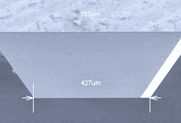
Deep Reactive Ion Etching (DRIE): Ensures uniformity <±5% and offers selectivity ratios exceeding 50:1, suitable for high-aspect-ratio silicon etching.
Reactive Ion Etching (RIE): Effective for etching silicon (Si), silicon dioxide (SiO₂), and silicon nitride (SiNx) with precise control.
Focused Ion Beam Etching (FIB): Enables micro- and nanoscale etching, deposition, and doping of materials and devices.
Inductively Coupled Plasma (ICP) Etching: Specialized for etching compound semiconductors, including GaN, GaAs, and InP.
