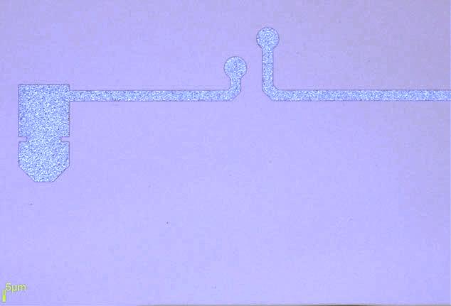
Our epitaxy and doping services provide precise control over material properties, essential for optimizing MEMS devices and semiconductor applications. Through advanced epitaxial growth and controlled doping techniques, we offer flexible solutions tailored to a wide range of materials and applications.
Metal-Organic Chemical Vapor Deposition (MOCVD): Enables the growth of high-quality epitaxial layers, ideal for materials like GaN and GaAs in optoelectronic and high-frequency applications.
Chemical Vapor Deposition (CVD): Supports epitaxial growth for materials such as SiC, suitable for high-power and high-temperature devices.
Ion Implantation: Provides precise doping capabilities for elements including boron (B), phosphorus (P), fluorine (F), aluminum (Al), nitrogen (N), argon (Ar), hydrogen (H), helium (He), and silicon (Si), allowing for customized electrical properties in semiconductor layers.
Additional high-temperature processes, such as Thermal Oxidation, High-Temperature Diffusion/Annealing, and Rapid Thermal Annealing (RTA), further enhance material performance and reliability.
©2025 Nano store