AFM, SEM, and Additional Analytical Services
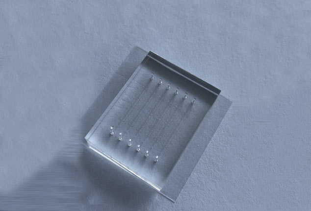
Our microfluidic device fabrication services utilize advanced lithography techniques from the microelectronics industry, combined with soft lithography for surface patterning, to create precise microchannel structures. To form fully functional microfluidic channels, we employ bonding techniques tailored to the materials used, including high-temperature, high-pressure, or high-voltage bonding for glass and silicon, and oxygen plasma bonding for […]
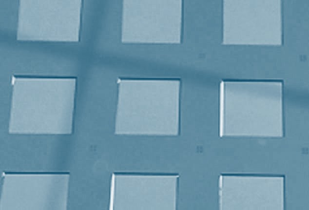
Custom silicon nitride (Si₃N₄) windows are ideal carriers for structural analysis and transmission imaging in synchrotron X-ray, soft X-ray, UV, and extreme UV applications. These thin-film windows provide exceptional thermal stability, enabling quasi-in-situ studies of sample morphology before and after annealing processes. Applications and Benefits: Versatile Sample Support: Suitable for TEM observation of materials and […]
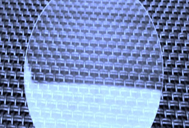
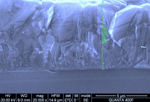
Our wafer thinning and polishing services ensure precise material reduction and surface refinement, essential for high-performance MEMS and semiconductor applications. Thinning removes excess material from the wafer’s backside, achieving the desired thickness for efficient packaging, while polishing reduces surface roughness to create a smooth, reflective finish. Thinning: Compatible with materials such as silicon (Si), gallium […]
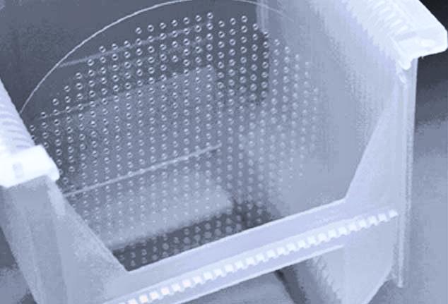
Our MEMS dicing and drilling services provide precise material separation and micro-hole fabrication for a wide range of applications, from semiconductor and LED chip manufacturing to medical and consumer electronics. Using advanced dicing and drilling techniques, we ensure accuracy and reliability for various substrate types and device requirements. Laser Dicing: Ideal for silicon substrates with […]
Our epitaxy and doping services provide precise control over material properties, essential for optimizing MEMS devices and semiconductor applications. Through advanced epitaxial growth and controlled doping techniques, we offer flexible solutions tailored to a wide range of materials and applications. Metal-Organic Chemical Vapor Deposition (MOCVD): Enables the growth of high-quality epitaxial layers, ideal for materials […]
Wafer bonding is a high-precision process that unites two meticulously cleaned, atomically smooth surfaces of either identical or different semiconductor materials. Through careful surface preparation and activation, wafers are bonded under controlled conditions using van der Waals forces, molecular interactions, or atomic bonding, resulting in a seamless, unified structure. We offer a range of advanced […]
Our MEMS thin-film deposition services offer high-quality coatings tailored for advanced applications in microelectronics, optoelectronics, and sensor technology. We provide a wide selection of both metallic and non-metallic materials, with deposition methods optimized for precision and consistency across various substrates. Deposition Materials: Metals: Ti, Al, Ni, Au, Ag, Cr, Pt, Cu, TiW (90), Pd, Zn, […]
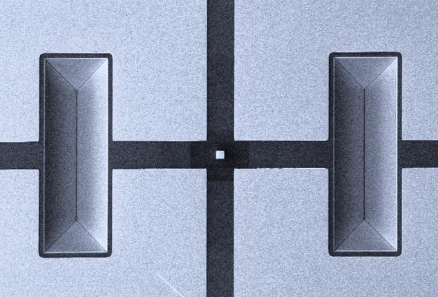
Etching is a critical process in MEMS fabrication, allowing for precise patterning and material removal across a range of substrates and material types. Our advanced etching capabilities include both chemical and physical methods to meet diverse application needs. We offer alkaline etching with KOH and TMAH, as well as acidic etching using HF, BOE, HCl, […]
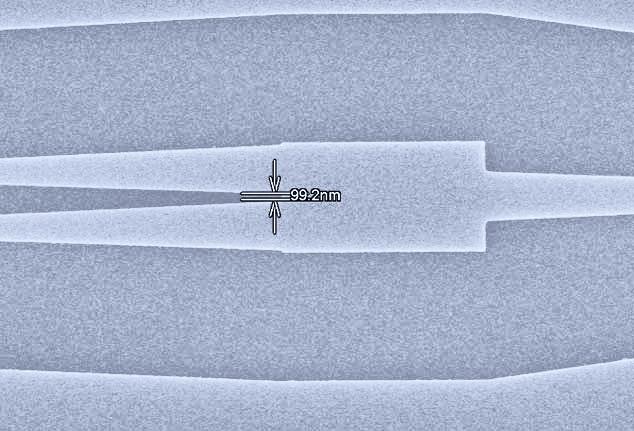
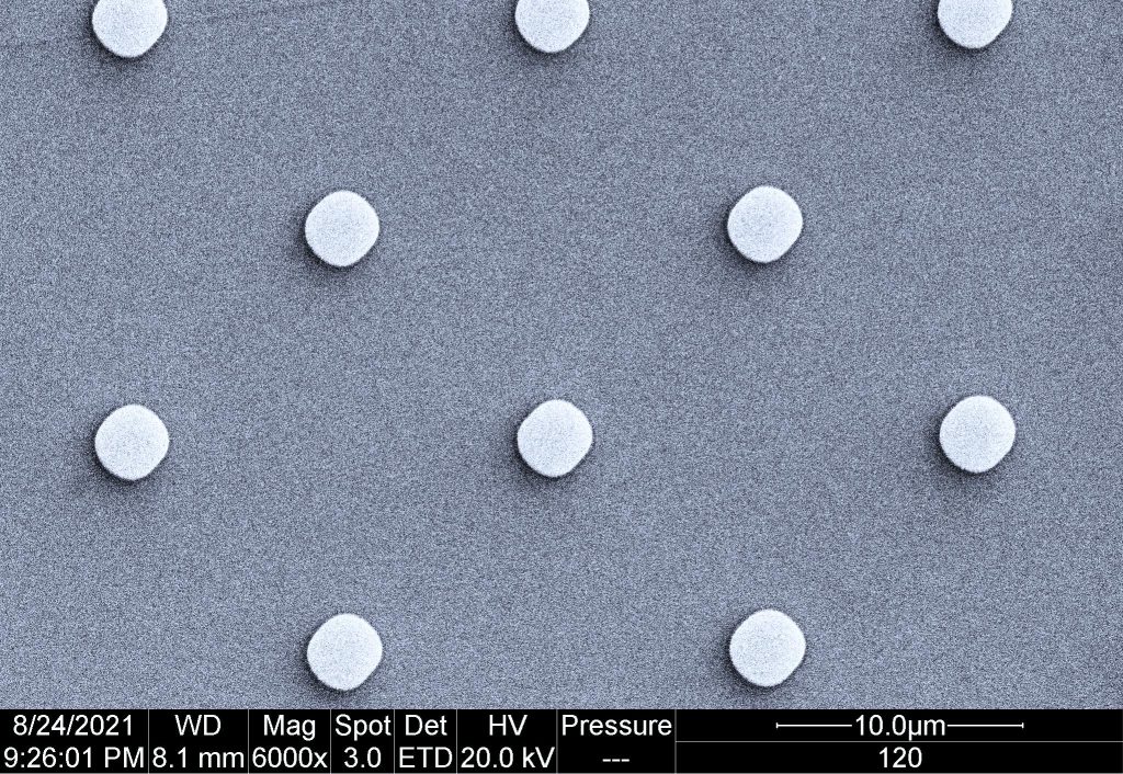
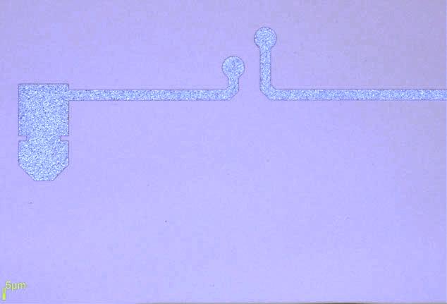
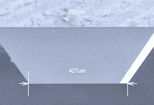
Photolithography is a cornerstone of semiconductor and MEMS fabrication, enabling precise patterning at the microscale and nanoscale. This advanced technique uses light to transfer intricate patterns onto wafer surfaces, creating openings in masking layers like silicon dioxide for localized impurity diffusion. Essential for defining device structures, photolithography allows for high-resolution patterning, layer alignment, and miniaturization, […]