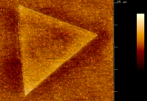
We offer a range of advanced characterization services tailored to meet the needs of researchers and industry professionals working with 2D materials, semiconductors, and nanomaterials. Our comprehensive suite of testing techniques includes Atomic Force Microscopy (AFM), Raman spectroscopy, fluorescence microscopy, and other analytical methods designed to provide detailed insights into material properties. AFM: Our AFM […]

Homojunction fabrication in 2D materials involves the sequential transfer of identical 2D materials, creating a layered structure with the same material. This process is particularly useful for applications that require enhanced material properties, such as increased active surface area or improved electronic coupling. In our wet transfer method, clients can choose the same 2D material, […]
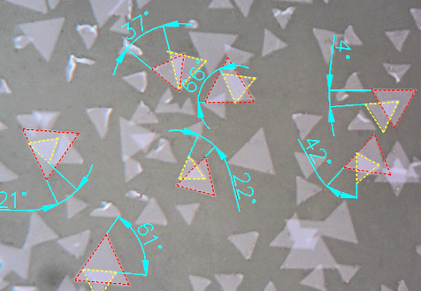
The fabrication of twisted-angle heterojunctions in 2D materials opens up opportunities for exploring novel electronic, optical, and quantum properties. This method involves selecting two different 2D materials and sequentially transferring them onto a substrate using a PMMA-assisted wet transfer technique. Through two consecutive transfers, a heterojunction is formed between the materials. Our process allows for […]
Mechanical exfoliation is an effective method for fabricating high-quality heterojunctions by transferring two distinct 2D materials, layer by layer, from bulk crystalline sources. This technique involves physically peeling thin layers of different bulk materials using adhesive tape (such as scotch tape) and then sequentially transferring them onto a chosen substrate to form a heterojunction. In […]
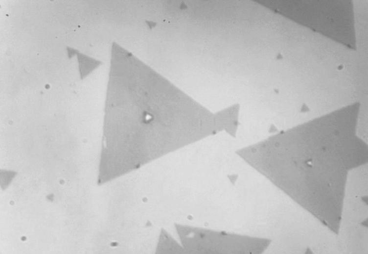
Mechanical exfoliation is a widely used method for obtaining high-quality monolayer or multilayer 2D materials directly from bulk crystals. Unlike chemical vapor deposition (CVD) or wet transfer techniques, this approach relies on the physical peeling of crystalline materials using adhesive tape, such as scotch tape, to isolate thin layers of the desired 2D material. In […]
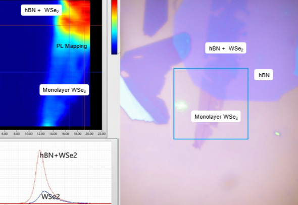
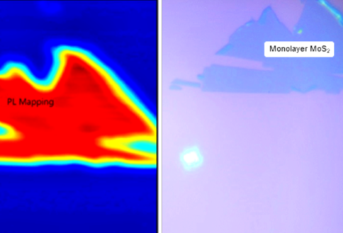
Monolayer and multilayer 2D materials are typically synthesized via Chemical Vapor Deposition (CVD) on specific substrates, such as sapphire, due to their favorable properties for growth. However, researchers and industry professionals often require these 2D materials to be integrated onto custom substrates for various applications. Our service offers precise wet transfer of 2D materials onto […]