Choose your ideal 2D material and preferred substrate.
Home > 2D Semiconctors > AFM, Raman, PL, SEM, and Additional Analytical Services
AFM, Raman, PL, SEM, and Additional Analytical Services
DESCRIPTION
We offer a range of advanced characterization services tailored to meet the needs of researchers and industry professionals working with 2D materials, semiconductors, and nanomaterials. Our comprehensive suite of testing techniques includes Atomic Force Microscopy (AFM), Raman spectroscopy, fluorescence microscopy, and other analytical methods designed to provide detailed insights into material properties.
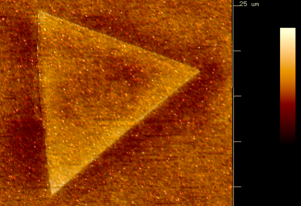
AFM: Our AFM services provide high-resolution imaging and surface analysis, allowing for the precise measurement of topography, surface roughness, and mechanical properties at the nanoscale.
Raman Spectroscopy: Raman analysis is essential for characterizing the vibrational modes of 2D materials, enabling phase identification, stress/strain analysis, and defect detection in materials such as graphene, MoS₂, and other layered compounds.
Photoluminescence Spectroscopy: Our PL spectroscopy services enable precise characterization of optical emission properties, providing essential insights into bandgap, defect states, and recombination processes in materials such as semiconductors, 2D materials, and nanostructures.