
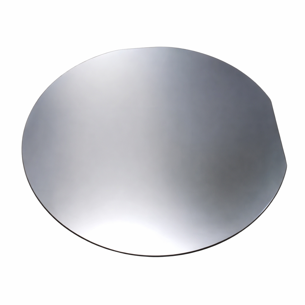
Nickel-Coated Silicon Wafers (Ni on Si (100))
Price range: د.إ606.08 through د.إ2,011.88
Nickel-Coated Silicon Wafers (Ni on Si (100))
Overview
Our nickel-coated silicon wafers are fabricated using high-vacuum magnetron sputtering to ensure uniform thickness, strong adhesion, and consistent surface quality applicable to electrochemical and materials research.
Nickel films are used in alkaline electrolysis, oxygen evolution reaction (OER), hydrogen evolution reaction (HER), and electrode development due to their high catalytic activity and corrosion resistance.
Layer Structure
Ni (Nickel layer)
Si (100) substrate
Optional adhesion layer available upon request:
Ti (5 nm)
Recommended Nickel Thickness
100 nm – * Recommended for general electrochemical research
200 nm – * Recommended for modified durability
500 nm – Thick conductive layer
1 µm – High-current or long-term testing applications
Substrate Specifications
Orientation: Si (100)
Doping: N-type, 1–10 Ω·cm resistivity
Surface finish: Single-side polished (SSP)
Custom options available upon request:
P-type silicon
Double-side polished (DSP)
Custom resistivity
Deposition Process
High-vacuum magnetron sputtering
Controlled thickness uniformity
Clean-room fits handling
Applications
Oxygen evolution reaction (OER)
Hydrogen evolution reaction (HER)
Electrochemical catalysis research
Electrode platform development
Electroplating and seed layer studies
Energy storage research
Quality & Packaging
Uniform film thickness control
Research-grade surface quality
Protective packaging to reduce oxidation exposure
Custom wafer sizes and thicknesses available upon request.
| Option 1 | 2″ Si | 100 nm Ni, 2″ Si | 200 nm Ni, 2″ Si | 500 nm Ni, 4″ Si | 100 nm Ni, 4″ Si | 200 nm Ni, 4″ Si | 500 nm Ni, 6″ Si | 100 nm Ni, 6″ Si | 200 nm Ni, 6″ Si | 500 nm Ni |
|---|
Related products
-
Nickel-Coated Silicon Substrates (Ni on Si (100))
Price range: د.إ157.85 through د.إ463.46