

Description
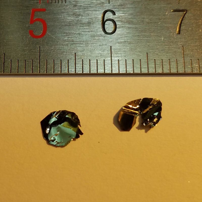
ZrSe₂ Crystals (Zirconium Diselenide)
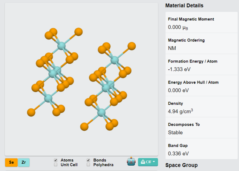
ZrSe₂ is a layered transition metal dichalcogenide (TMD) with a van der Waals structure, known for its excellent electronic, optical, and catalytic properties. It exhibits semiconducting behavior with an indirect bandgap, making it highly suitable for applications in nanoelectronics, optoelectronics, energy storage, and catalysis. Our ZrSe₂ crystals are synthesized using the Chemical Vapor Transport (CVT) method, ensuring high purity, precise stoichiometry, and superior crystallinity.
Sample Size Options:
Crystals larger than 10 mm²
Crystals larger than 25 mm²
Crystals larger than 100 mm²
Material Properties:
Layered Van der Waals Structure: Facilitates easy exfoliation into monolayers or few-layer nanosheets for 2D materials research.
Semiconducting Behavior: Suitable for electronic and optoelectronic devices.
High Carrier Mobility: Ideal for field-effect transistors (FETs) and nanoelectronic applications.
Strong Optical Absorption: Excellent absorption properties in the visible and near-infrared spectrum, making it suitable for photodetectors and solar cells.
Thermal and Chemical Stability: High environmental stability, ensuring long-term performance in various device applications.
Crystal Structure:
Type: Hexagonal layered structure (2H phase)
Features: High crystallinity with uniform, defect-free layers, ideal for thin-film fabrication and nanoscale device applications.
Degree of Exfoliation:
Ease of Use: Easily exfoliated into monolayers or few-layer nanosheets for advanced materials research and heterostructure integration.
Other Characteristics:
Anisotropic Transport Properties: Direction-dependent electronic and thermal conductivity, useful for advanced device architectures.
High Dielectric Constant: Suitable for use in next-generation high-κ dielectric materials.
Energy Band Engineering: Tunable electronic properties through doping, strain, or layer thickness control.
Applications:
Nanoelectronics:
High-performance material for transistors, logic devices, and flexible electronics.
Optoelectronics:
Ideal for photodetectors, light-emitting diodes (LEDs), and photovoltaic devices.
Energy Storage:
Potential applications in lithium-ion batteries, supercapacitors, and hydrogen evolution reactions (HER).
2D Material Studies:
Perfect for exfoliation into monolayers and integration into van der Waals heterostructures.
Sensors:
High sensitivity for gas detection, biosensing, and chemical sensing applications.
Synthesis Method:
Chemical Vapor Transport (CVT): Ensures high-quality crystals with excellent purity, uniform thickness, and superior structural integrity.
Additional information
| CAS Number | 121₆₆-4₇-1 |
|---|