CUSTOM 2D SEMICONDUCTOR PRODUCTS

Choose your ideal 2D material and preferred substrate.

Home > Custom Products

Wet Transfer of Monolayer/Multilayer 2D Materials

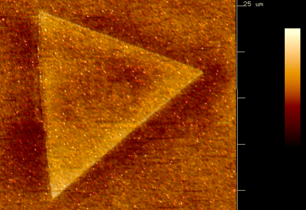
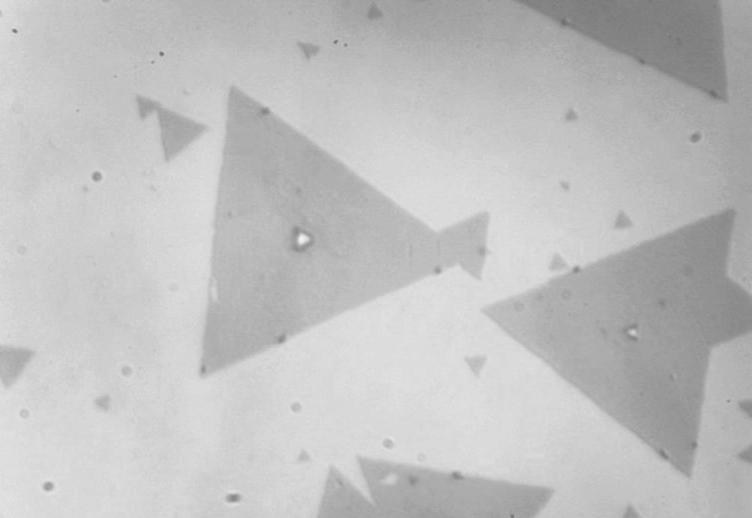
Monolayer and multilayer 2D materials are typically synthesized via Chemical Vapor Deposition (CVD) on specific substrates, such as sapphire, due to their favorable properties for growth. However, researchers and industry professionals often require these 2D materials to be integrated onto custom substrates for various applications. Our service offers precise wet transfer of 2D materials onto the substrate of your choice. Utilizing a PMMA (polymethyl methacrylate) layer and wet chemical transfer techniques, we can successfully transfer monolayer or multilayer 2D materials onto a wide range of substrates, including PET (polyethylene terephthalate), PI (polyimide), ITO (indium tin oxide), FTO (fluorine-doped tin oxide), glass, metal substrates, and more. This transfer process ensures that the material retains its integrity and properties while allowing you to explore new device architectures and applications on substrates tailored to your specific research or production needs.

Mechanical Exfoliation of Monolayer /Multilayer 2D Materials

Mechanical exfoliation is a widely used method for obtaining high-quality monolayer or multilayer 2D materials directly from bulk crystals. Unlike chemical vapor deposition (CVD) or wet transfer techniques, this approach relies on the physical peeling of crystalline materials using adhesive tape, such as scotch tape, to isolate thin layers of the desired 2D material. In this process, a bulk crystal (e.g., MoS₂, WS₂, or graphene) is carefully peeled using the tape, and the exfoliated material is then transferred onto the client’s selected substrate. This method is effective for producing pristine monolayer or multilayer regions and offers high crystallinity, making it ideal for fundamental research and device prototyping. We provide mechanical exfoliation services on a wide range of substrates, such as PET, PI, ITO, FTO, glass, metals, and others, allowing researchers to integrate 2D materials into flexible, transparent, or conductive devices. This technique is particularly valued for applications in nanoscale electronics, photonics, and catalysis, where the intrinsic properties of the 2D material need to be preserved. Mechanical exfoliation enables clients to access high-quality 2D material samples tailored to their specific substrate needs, ensuring they can explore novel properties and applications in their research or product development.

Mechanical Exfoliation for Heterojunction Fabrication

Mechanical exfoliation is an effective method for fabricating high-quality heterojunctions by transferring two distinct 2D materials, layer by layer, from bulk crystalline sources. This technique involves physically peeling thin layers of different bulk materials using adhesive tape (such as scotch tape) and then sequentially transferring them onto a chosen substrate to form a heterojunction. In this process, we start by mechanically exfoliating a layer of the first 2D material, such as MoS₂, WS₂, or graphene, and transferring it onto the client’s selected substrate. After the first layer is successfully placed, a second 2D material is exfoliated and carefully aligned on top of the first layer, creating the desired heterojunction structure. This process is flexible and can be performed on a variety of substrates, including PET, PI, ITO, FTO, glass, metal substrates, and others. The heterojunctions created through mechanical exfoliation exhibit high crystallinity and strong interlayer interactions, making them ideal for applications in electronic, optoelectronic, and energy-harvesting devices. This method preserves the intrinsic properties of the individual materials while enabling the exploration of novel electronic and optical phenomena that arise from the heterostructure. Our mechanical exfoliation service for heterojunction fabrication offers a reliable and versatile solution for researchers and innovators looking to create high-quality 2D material heterojunctions on their preferred substrates.

Wet Transfer for Twisted-Angle Heterojunction Fabrication

The fabrication of twisted-angle heterojunctions in 2D materials opens up opportunities for exploring novel electronic, optical, and quantum properties. This method involves selecting two different 2D materials and sequentially transferring them onto a substrate using a PMMA-assisted wet transfer technique. Through two consecutive transfers, a heterojunction is formed between the materials. Our process allows for the transfer of these 2D materials onto a wide range of substrates, including PET (polyethylene terephthalate), PI (polyimide), ITO (indium tin oxide), FTO (fluorine-doped tin oxide), glass, metal substrates, and more. This flexible approach enables the integration of 2D heterojunctions into various device platforms, including flexible, transparent, or conductive systems, among others. Twisted-angle heterojunctions have diverse applications in advanced electronic and optoelectronic devices, such as high-performance transistors, photodetectors, and energy-harvesting technologies. These heterojunctions are also valuable for investigating quantum phenomena and tunable properties arising from interlayer interactions. With our wet transfer service for twisted-angle heterojunction fabrication, we provide a robust platform for researchers and innovators to explore the vast potential of 2D material systems on their chosen substrates.

Wet Transfer for Homojunction Fabrication

Homojunction fabrication in 2D materials involves the sequential transfer of identical 2D materials, creating a layered structure with the same material. This process is particularly useful for applications that require enhanced material properties, such as increased active surface area or improved electronic coupling. In our wet transfer method, clients can choose the same 2D material, such as MoS₂, to fabricate a homojunction. For example, the process could involve transferring a larger MoS₂ layer, followed by a smaller MoS₂ layer (as illustrated in the image). This technique uses a PMMA-assisted wet transfer approach to ensure smooth and accurate transfers onto a variety of substrates, such as PET, PI, ITO, FTO, glass, metals, etc. Homojunctions have applications in electronic devices, optoelectronics, and catalysis, where uniform material composition is essential for consistent performance. This fabrication process allows for the precise layering of identical materials, enabling the exploration of novel device architectures and enhanced functionalities in 2D material systems. Our wet transfer service for homojunction fabrication offers flexibility and control, allowing clients to integrate homojunctions onto their preferred substrates and take advantage of the unique properties that come with layered 2D materials.

AFM, Raman, PL, SEM, and Additional Analytical Services

We offer a range of advanced characterization services tailored to meet the needs of researchers and industry professionals working with 2D materials, semiconductors, and nanomaterials. Our comprehensive suite of testing techniques includes Atomic Force Microscopy (AFM), Raman spectroscopy, fluorescence microscopy, and other analytical methods designed to provide detailed insights into material properties. AFM: Our AFM services provide high-resolution imaging and surface analysis, allowing for the precise measurement of topography, surface roughness, and mechanical properties at the nanoscale. Raman Spectroscopy: Raman analysis is essential for characterizing the vibrational modes of 2D materials, enabling phase identification, stress/strain analysis, and defect detection in materials such as graphene, MoS₂, and other layered compounds. Photoluminescence Spectroscopy: Our PL spectroscopy services enable precise characterization of optical emission properties, providing essential insights into bandgap, defect states, and recombination processes in materials such as semiconductors, 2D materials, and nanostructures.